ADS1299
SBAS499A –JULY 2012–REVISED AUGUST 2012
www.ti.com
Input Common-Mode Range
The usable input common-mode range of the front-end depends on various parameters, including the maximum
differential input signal, supply voltage, PGA gain, and so forth. This range is described in Equation 2:
Gain VMAX_DIFF
2
Gain VMAX_DIFF
2
AVDD - 0.2 -
> CM > AVSS + 0.2 +
where:
VMAX_DIFF = maximum differential signal at the PGA input
CM = common-mode range
(2)
For example:
If VDD = 5 V, gain = 12, and VMAX_DIFF = 350 mV
Then 2.3 V < CM < 2.7 V
Input Differential Dynamic Range
The differential (INP – INN) signal range depends on the analog supply and reference used in the system. This
range is shown in Equation 3.
VREF
±VREF
2 VREF
Max (INP - INN) <
;
Full-Scale Range =
=
Gain
Gain
Gain
(3)
The 5-V supply, with a reference of 4.5 V and a gain of 12 for EEGs, is optimized for power with a differential
input signal of approximately 300 mV.
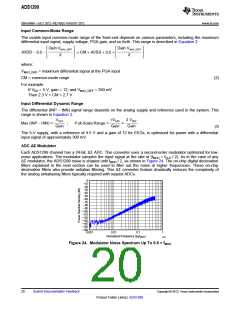
ADC ΔΣ Modulator
Each ADS1299 channel has a 24-bit, ΔΣ ADC. This converter uses a second-order modulator optimized for low-
noise applications. The modulator samples the input signal at the rate of (fMOD = fCLK / 2). As in the case of any
ΔΣ modulator, the ADS1299 noise is shaped until fMOD / 2, as shown in Figure 24. The on-chip digital decimation
filters explained in the next section can be used to filter out the noise at higher frequencies. These on-chip
decimation filters also provide antialias filtering. This ΔΣ converter feature drastically reduces the complexity of
the analog antialiasing filters typically required with nyquist ADCs.
0
−10
−20
−30
−40
−50
−60
−70
−80
−90
−100
−110
−120
−130
−140
−150
−160
0.001
0.01
0.1
1
Normalized Frequency (fIN/fMOD
)
G001
Figure 24. Modulator Noise Spectrum Up To 0.5 × fMOD
20
Submit Documentation Feedback
Copyright © 2012, Texas Instruments Incorporated
Product Folder Link(s): ADS1299

 TI [ TEXAS INSTRUMENTS ]