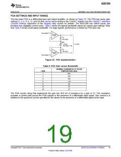
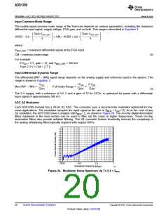
ADS1299
www.ti.com
SBAS499A –JULY 2012–REVISED AUGUST 2012
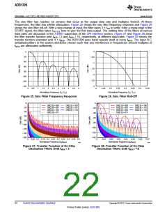
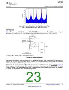
0
−20
−40
−60
−80
−100
−120
−140
0
0.5
1
1.5
2
2.5
3
3.5
4
Normalized Frequency (fIN/fMOD
)
G029
Figure 29. Transfer Function of On-Chip Decimation Filters
Until 4 fMOD for DR[2:0] = 000 and DR[2:0] = 110
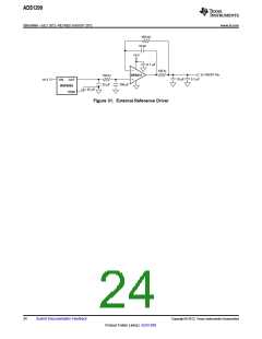
REFERENCE
Figure 30 shows a simplified block diagram of the ADS1299 internal reference. The 4.5-V reference voltage is
generated with respect to AVSS. When using the internal voltage reference, connect VREFN to AVSS.
100 mF
VCAP1
R1(1)
Bandgap
4.5 V
VREFP
R3(1)
10 mF
R2(1)
VREFN
AVSS
To ADC Reference Inputs
(1) For VREF = 4.5 V: R1 = 9.8 kΩ, R2 = 13.4 kΩ, and R3 = 36.85 kΩ.
Figure 30. Internal Reference
The external band-limiting capacitors determine the amount of reference noise contribution. For high-end EEG
systems, the capacitor values should be chosen such that the bandwidth is limited to less than 10 Hz so that the
reference noise does not dominate system noise.
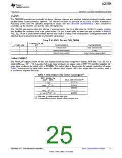
Alternatively, the internal reference buffer can be powered down and VREFP can be applied externally. Figure 31
shows a typical external reference drive circuitry. Power-down is controlled by the PD_REFBUF bit in the
CONFIG3 register. This power-down is also used to share internal references when two devices are cascaded.
By default, the device wakes up in external reference mode.
Copyright © 2012, Texas Instruments Incorporated
Submit Documentation Feedback
23
Product Folder Link(s): ADS1299

 TI [ TEXAS INSTRUMENTS ]