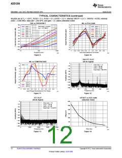
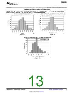
ADS1299
SBAS499A –JULY 2012–REVISED AUGUST 2012
www.ti.com
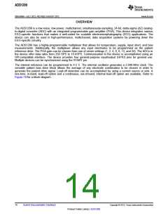
THEORY OF OPERATION
This section contains details of the ADS1299 internal functional elements. The analog blocks are discussed first,
followed by the digital interface. Blocks implementing EEG-specific functions are covered at the end of this
document.
Throughout this document, fCLK denotes the CLK pin signal frequency, tCLK denotes the CLK pin signal period,
fDR denotes the output data rate, tDR denotes the output data time period, and fMOD denotes the frequency at
which the modulator samples the input.
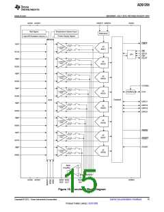
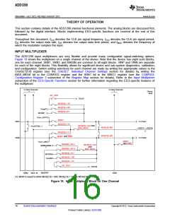
INPUT MULTIPLEXER
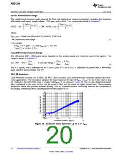
The ADS1299 input multiplexers are very flexible and provide many configurable signal-switching options.
Figure 19 shows the multiplexer on a single channel of the device. Note that the device has eight such blocks,
one for each channel. SRB1, SRB2, and BIASIN are common to all eight blocks. VINP and VINN are separate
for each of the eight blocks. This flexibility allows for significant device and sub-system diagnostics, calibration,
and configuration. Switch setting selections for each channel are made by writing the appropriate values to the
CHnSET[3:0] register (see the CHnSET: Individual Channel Settings section for details) by writing the
BIAS_MEAS bit in the CONFIG3 register and the SRB1 bit in the MISC1 register (see the CONFIG3:
Configuration Register 3 subsection of the Register Map section for details). Refer to the Input Multiplexer
subsection of the EEG-Specifc Functions section for further information regarding the EEG-specific features of
the multiplexer.
To Next Channels
To Next Channels
Device
MUX
INT_TEST
TESTP
MUX[2:0] = 101
MUX[2:0] =100
MUX[2:0] =011
TempP
MVDDP
From LOFFP
MAIN(1)
To PGAP
VINP
VINN
MUX[2:0] =110
MUX[2:0] = 010 AND
BIAS_MEAS
CHxSET[3] = 1
MUX[2:0] =001
(VREFP + VREFN)
2
MUX[2:0] =111
MUX[2:0] =001
MAIN(1) AND SRB1
To PGAN
MAIN(1)
AND SRB1
From LoffN
(AVDD+AVSS)
BIASREF_INT=1
BIASREF_INT=0
MUX[2:0] = 010
AND
BIAS_MEAS
2
MUX[2:0] = 011
MUX[2:0] = 100
MUX[2:0] = 101
MVDDN
TempN
INT_TEST
TESTM
BIASREF
SRB2
BIAS_IN
SRB1
(1) MAIN is equal to either MUX[2:0] = 000, MUX[2:0] = 110, or MUX[2:0] = 111.
Figure 19. Input Multiplexer Block for One Channel
16
Submit Documentation Feedback
Copyright © 2012, Texas Instruments Incorporated
Product Folder Link(s): ADS1299

 TI [ TEXAS INSTRUMENTS ]