ADS1115-Q1
www.ti.com
SBAS563 –DECEMBER 2011
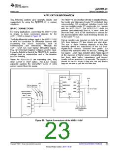
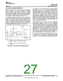
LOW-SIDE CURRENT MONITOR
The ADS1115-Q1 are fabricated in a small-geometry,
low-voltage process. The analog inputs feature
protection diodes to the supply rails. However, the
current-handling ability of these diodes is limited, and
the ADS1115-Q1 can be permanently damaged by
analog input voltages that remain more than
approximately 300mV beyond the rails for extended
periods. One way to protect against overvoltage is to
place current-limiting resistors on the input lines. The
ADS1115-Q1 analog inputs can withstand momentary
currents as large as 100mA.
Figure 38 shows a circuit for a low-side shunt-type
current monitor. The circuit monitors the voltage
across a shunt resistor, which is sized as small as
possible while giving a measurable output voltage.
This voltage is amplified by an OPA335 low-drift op
amp, and the result is read by the ADS1115-Q1.
It is suggested that the ADS1115-Q1 be operated at
a gain of 8. The gain of the OPA335 can then be set
lower. For a gain of 16, the op amp should be set up
to give a maximum output voltage no greater than
0.256V. If the shunt resistor is sized to provide a
maximum voltage drop of 50mV at full-scale current,
the full-scale input to the ADS1115-Q1 is 0.2V.
If the ADS1115-Q1 are driven by an op amp with
high-voltage supplies, such as ±12V, protection
should be provided, even if the op amp is configured
so that it does not output out-of-range voltages. Many
op amps drift to one of the supply rails immediately
when power is applied, usually before the input has
stabilized; this momentary spike can damage the
ADS1115-Q1. This incremental damage results in
slow, long-term failure, which can be disastrous for
permanently installed, low-maintenance systems.
2.0V to 5V
3kW
0.1mF Typ
V
5V
FS = 0.2V
Load
OPA335
(1)
R3
If an op amp or other front-end circuitry is used with
an ADS1115-Q1, performance characteristics must
be taken into account when designing the application.
I2C
ADS1115-Q1
49.9kW
(2)
RS
1kW
-5V
G = 4
(PGA Gain = 16)
256mV FS
(1) Pull-down resistor to allow accurate swing
to 0V.
(2) RS is sized for a 50mV drop at full-scale
current.
Figure 38. Low-Side Current Measurement
Copyright © 2011, Texas Instruments Incorporated
Submit Documentation Feedback
27
Product Folder Link(s) :ADS1115-Q1

 TI [ TEXAS INSTRUMENTS ]