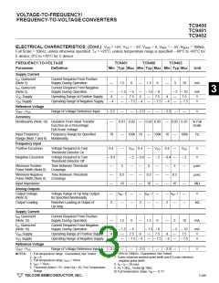
VOLTAGE-TO-FREQUENCY/
FREQUENCY-TO-VOLTAGECONVERTERS
1
2
3
4
5
6
7
8
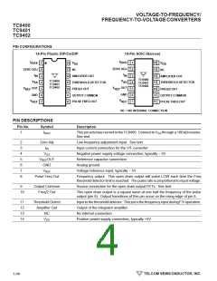
TC9400
TC9401
TC9402
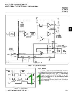
Output Common
VREF Out
The sources of both the Freq/2 out and the Pulse Freq
Out are connected to this pin. An output level swing from the
drainvoltagetogroundortotheVSS supplymaybeobtained
by connecting this pin to the appropriate point.
The charging current for CREF is supplied through this
pin. When the op amp output reaches the threshold level,
this pin is internally connected to the reference voltage and
a charge, equal to VREF x CREF, is removed from the
integrator capacitor. After about 3 µsec, this pin is internally
connected to the summing junction of the op amp to dis-
charge CREF. Break-before-make switching ensures that
the reference voltage is not directly applied to the summing
junction.
RBIAS
An external resistor, connected to VSS, sets the bias
point for the TC9400. Specifications for the TC9400 are
based on RBIAS = 100kΩ ±10%, unless otherwise noted.
Increasing the maximum frequency of the TC9400
beyond 100kHz is limited by the pulse width of the Pulse
Output (typically 3µsec). Reducing RBIAS will decrease the
pulsewidthandincreasethemaximumoperatingfrequency,
but linearity errors will also increase. RBIAS can be reduced
to 20kΩ, which will typically produce a maximum full scale
frequency of 500kHz.
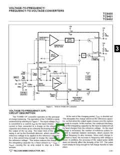
V/F CONVERTER DESIGN INFORMATION
Input/Output Relationships
Theoutputfrequency(fOUT)isrelatedtotheanaloginput
voltage (VIN) by the transfer equation:
VIN
RIN
1
Frequency out =
×
(VREF) (CREF
)
Amplifier Out
External Component Selection
The output stage of the operational amplifier. During
V/F operation, a negative-going ramp signal is available at
this pin. In the F/V mode, a voltage proportional to the
frequency input is generated.
RIN
The value of this component is chosen to give a full-
scale input current of approximately 10µA:
Zero Adjust
VIN Full Scale
RIN
.
10µA
10V
This pin is the noninverting input of the operational
amplifier. The low-frequency set point is determined by
adjusting the voltage at this pin.
Example:
RIN
= 1MΩ.
10µA
Note that the value is an approximation and the exact
relationship is defined by the transfer equation. In practice,
the value of RIN typically would be trimmed to obtain full-
scale frequency at VIN full scale (see "Adjustment Proce-
dure"). Metal film resistors with 1% tolerance or better are
recommended for high-accuracy applications because of
their thermal stability and low-noise generation.
IIN
The inverting input of the operational amplifier and the
summing junction when connected in the V/F mode. An
input current of 10µA is specified, but an overrange current
up to 50µA can be used without detrimental effect to the
circuit operation. IIN connects the summing junction of an
operational amplifier. Voltage sources cannot be attached
directly, but must be buffered by external resistors.
CINT
The exact value is not critical but is related to CREF by
the relationship:
VREF
Areferencevoltagefromeitheraprecisionsourceorthe
VSS supply is applied to this pin. Accuracy of the TC9400 is
dependent on the voltage regulation and temperature char-
acteristics of the reference circuitry.
Since the TC9400 is a charge balancing V/F converter,
the reference current will be equal to the input current. For
this reason, the DC impedance of the reference voltage
source must be kept low enough to prevent linearity errors.
For linearity of 0.01%, a reference impedance of 200Ω or
less is recommended. A 0.1µF bypass capacitor should be
connected from VREF to ground.
3CREF ≤ CINT ≤ 10 CREF
.
Improved stability and linearity are obtained when
CINT ≤ 4CREF. Low-leakage types are recommended,
although mica and ceramic devices can be used in applica-
tions where their temperature limits are not exceeded.
Locate as close as possible to pins 12 and 13.
TELCOM SEMICONDUCTOR, INC.
3-293

 TELCOM [ TELCOM SEMICONDUCTOR, INC ]