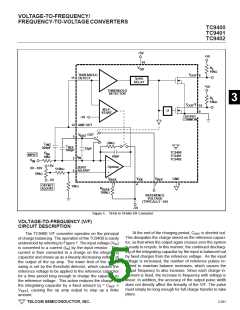
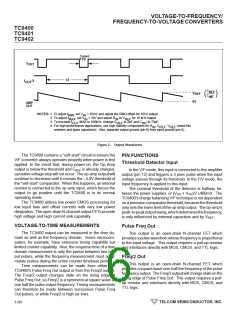
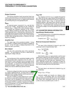
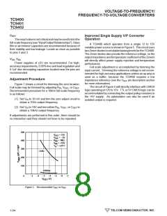
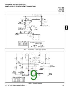
VOLTAGE-TO-FREQUENCY/
FREQUENCY-TO-VOLTAGECONVERTERS
1
2
3
4
5
6
7
8
TC9400
TC9401
TC9402
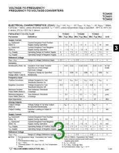
ELECTRICAL CHARACTERISTICS: (Cont.) VDD = +5V, VSS = – 5V, VGND = 0, VREF = – 5V, RBIAS = 100kΩ,
Full Scale = 10kHz, unless otherwise specified. TA = +25°C, unless temperature range is specified – 40°C to +85°C for
E device, 0°C to +70°C for C device.
FREQUENCY-TO-VOLTAGE
TC9401
TC9400
TC9402
Parameter
Definition
Min Typ Max Min Typ Max Min Typ Max
Unit
Supply Current
IDD Quiescent
(Note 5)
Current Required From Positive
Supply During Operation
—
1.5
6
—
1.5
6
—
4
3
10
mA
ISS Quiescent
(Note 5)
Current Required From Negative
Supply During Operation
—
4
– 1.5 – 6
—
4
– 1.5 – 6
– 3 – 10
mA
V
VDD Supply
VSS Supply
Operating Range of Positive Supply
Operating Range of Negative Supply
—
—
7.5
—
—
7.5
—
—
7.5
– 4
– 7.5 – 4
– 7.5 – 4
– 7.5
V
Reference Voltage
VREF –VSS
Range of Voltage Reference Input
– 2.5
—
—
—
– 2.5
—
—
—
– 2.5
—
—
—
V
Accuracy
Nonlinearity (Note 10) Deviation From Ideal Transfer
Function as a Percentage
0.01 0.02
0.02 0.05
0.05 0.25
% Full
Scale
Full-Scale Voltage
Input Frequency
Frequency Range for Specified
10
—
—
100k 10
—
100k 10
—
100k
Hz
Range (Note 7 and 8) Nonlinearity
Frequency Input
Positive Excursion
Voltage Required to Turn
Threshold Detector On
0.4
– 0.4
—
VDD 0.4
– 2 – 0.4
—
—
5
VDD 0.4
—
VDD
– 2
—
V
Negative Excursion
Voltage Required to Turn
Threshold Detector Off
– 2 – 0.4 —
V
Minimum Positive
Pulse Width (Note 8)
Time Between Threshold
Crossings
5
—
—
—
—
—
—
—
—
—
—
—
—
5
µsec
µsec
MΩ
Minimum Negative
Pulse Width (Note 8)
Time Between Threshold
Crossings
—
0.5
10
0.5
10
0.5
10
Input Impedance
—
—
Analog Outputs
Output Voltage
(Note 9)
Voltage Range of Op Amp Output
for Specified Nonlinearity
—
2
VDD – 1
—
—
2
VDD – 1
—
—
2
VDD – 1
—
—
V
Output Loading
Resistive Loading at Output of
Op Amp
—
—
—
—
—
kΩ
Supply Current
IDD Quiescent
(Note 10)
Current Required From Positive
Supply During Operation
—
1.5
6
—
4
1.5
6
—
4
3
10
mA
ISS Quiescent
(Note 10)
Current Required From Negative
Supply During Operation
—
4
– 1.5 – 6
– 1.5 – 6
– 3 – 10
mA
V
VDD Supply
VSS Supply
Operating Range of Positive Supply
Operating Range of Negative Supply
—
—
7.5
—
—
7.5
—
—
7.5
– 4
– 7.5 – 4
– 7.5 – 4
– 7.5
V
Reference Voltage
VREF –VSS
Range of Voltage Reference Input
– 2.5
—
—
– 2.5
—
—
– 2.5 —
—
V
6. 10Hz to 100kHz.; Guaranteed, Not Tested
NOTES: 1. Full temperature range. Guaranteed, Not Tested.
2. IIN = 0.
7. 5µsec minimum positive pulse width and 0.5 µsec minimum
negative pulse width.
8. tR = tF = 20 nsec.
3. Full temperature range, IOUT = 10mA.
4. IOUT = 10µA.
5. Threshold Detect = 5V, Amp Out = 0V, Full Temperature
Range
9. RL ≥ 2kΩ.; Tested @ 10kΩ
10. Full temperature range, VIN = – 0.1V.
TELCOM SEMICONDUCTOR, INC.
3-289

 TELCOM [ TELCOM SEMICONDUCTOR, INC ]