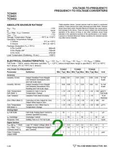
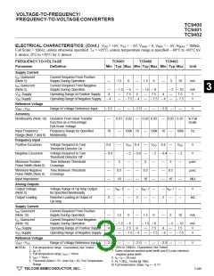
VOLTAGE-TO-FREQUENCY/
FREQUENCY-TO-VOLTAGECONVERTERS
TC9400
TC9401
TC9402
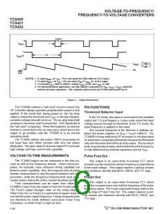
3 µsec
TYP
f
OUT
1/f
f
/2
OUT
C
REF
INT
V
REF
C
0V
AMP
OUT
NOTES: 1. To adjust f
, set V = 10mV and adjust the 50kΩ offset for 10Hz output.
MIN
IN
2. To adjust f
3. To increase f
, set V = 10V and adjust R or V
for 10 kHz output.
MAX
IN
IN
REF
to 2pF and C
MAX to 100kHz, change C
to 75pF.
OUT
REF
INT
4. For high-performance applications, use high-stability components for R , C
resistors and glass capacitors). Also, separate output ground (pin 9) from input ground (pin 6).
, V
(metal film
IN REF REF
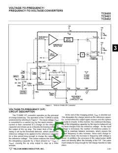
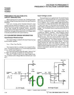
Figure 2 . Output Waveforms
The TC9400 contains a "self-start" circuit to ensure the
V/F converter always operates properly when power is first
applied. In the event that, during power-on, the Op Amp
output is below the threshold and CREF is already charged,
apositivevoltagestepwillnotoccur. Theop-ampoutputwill
continue to decrease until it crosses the –3.0V threshold of
the "self-start" comparator. When this happens, an internal
resistor is connected to the op-amp input, which forces the
output to go positive until the TC9400 is in its normal
operating mode.
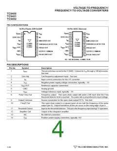
PIN FUNCTIONS
Threshold Detector Input
In the V/F mode, this input is connected to the amplifier
output (pin 12) and triggers a 3 µsec pulse when the input
voltage passes through its threshold. In the F/V mode, the
input frequency is applied to this input.
The nominal threshold of the detector is halfway be-
tween the power supplies, or (VDD + VSS)/2 ±400mV. The
TC9400's charge balancing V/F technique is not dependent
on a precision comparator threshold, because the threshold
only sets the lower limit of the op-amp output. The op-amp's
peak-to-peakoutputswing,whichdeterminesthefrequency,
The TC9400 utilizes low power CMOS processing for
low input bias and offset currents with very low power
dissipation. Theopen-drainN-channeloutputFETsprovide
high voltage and high current sink capability.
is only influenced by external capacitors and by VREF
.
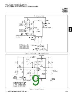
VOLTAGE-TO-TIME MEASUREMENTS
Pulse Freq Out
The TC9400 output can be measured in the time do-
main as well as the frequency domain. Some microcom-
puters, for example, have extensive timing capability but
limited counter capability. Also, the response time of a time
domain measurement is only the period between two out-
put pulses, while the frequency measurement must accu-
mulate pulses during the entire counter timebase period.
Time measurements can be made from either the
TC9400's Pulse Freq Out output or from the Freq/2 output.
The Freq/2 output changes state on the rising edge of
Pulse Freq Out, so Freq/2 is a symmetrical square wave at
one half the pulse output frequency. Timing measurements
can therefore be made between successive Pulse Freq
Out pulses, or while Freq/2 is high (or low).
This output is an open-drain N-channel FET which
provides a pulse waveform whose frequency is proportional
to the input voltage. This output requires a pull-up resistor
and interfaces directly with MOS, CMOS, and TTL logic.
Freq/2 Out
This output is an open-drain N-channel FET which
provides a square wave one-half the frequency of the pulse
frequencyoutput. TheFreq/2outputwillchangestateonthe
rising edge of Pulse Freq Out. This output requires a pull-
up resistor and interfaces directly with MOS, CMOS, and
TTL logic.
3-292
TELCOM SEMICONDUCTOR, INC.

 TELCOM [ TELCOM SEMICONDUCTOR, INC ]