VOLTAGE-TO-FREQUENCY/
FREQUENCY-TO-VOLTAGECONVERTERS
TC9400
TC9401
TC9402
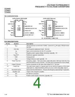
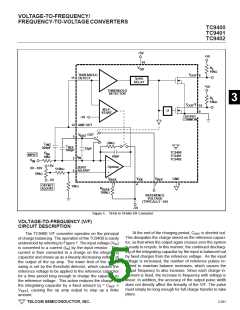
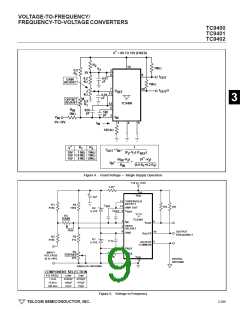
PIN CONFIGURATIONS
14-Pin Plastic DIP/CerDIP
14-Pin SOIC (Narrow)
I
I
BIAS
14
13
12
V
1
2
3
4
5
6
7
V
DD
BIAS
1
2
3
4
5
6
7
14
13
12
DD
ZERO ADJ
ZERO ADJ
NC
NC
I
I
IN
AMPLIFIER OUT
IN
AMPLIFIER OUT
TC9400
TC9401
TC9402
V
TC9400
TC9401
TC9402
V
SS
11 THRESHOLD DETECTOR
10 FREQ/2 OUT
SS
11 THRESHOLD DETECTOR
10 FREQ/2 OUT
V
OUT
GND
V
OUT
GND
REF
REF
9
8
OUTPUT COMMON
PULSE FREQ OUT
9
8
OUTPUT COMMON
PULSE FREQ OUT
V
V
REF
REF
NC = NO INTERNAL CONNECTION
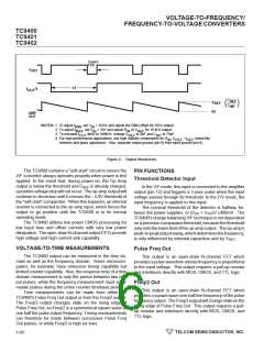
PIN DESCRIPTIONS
Pin No.
Symbol
Description
1
IBIAS
ThispinsetsbiascurrentintheTC9400. ConnecttoVSS througha100kΩ resistor.
See text.
2
3
4
5
6
7
8
Zero Adj
IIN
Low frequency adjustment input. See text.
Input current connection for the V/F converter.
Negative power supply voltage connection, typically – 5V.
Reference capacitor connection.
VSS
VREFOUT
GND
Analog ground.
VREF
Voltage reference input, typically – 5V.
Pulse Freq Out
Frequency output. This open drain output will pulse LOW each time the Freq
threshold detector limit is reached. The pulse rate is proportional to input voltage.
9
Output Common
Freq/2 Out
Source connection for the open drain output FETs. See text.
10
This open drain output is a square wave at one half the frequency of the pulse
output (pin 8). Output transitions of this pin occur on the rising edge of pin 8.
11
12
13
14
Threshold Detect
Amplifier Out
NC
Inputtothethresholddetector. ThispinisthefrequencyinputduringF/Voperation.
Output of the integrator amplifier.
No internal connection
VDD
Positive power supply connection, typically +5V.
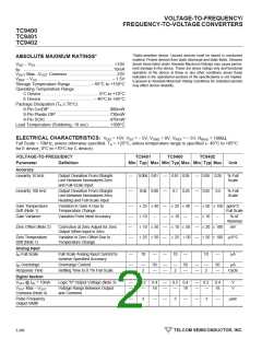
3-290
TELCOM SEMICONDUCTOR, INC.

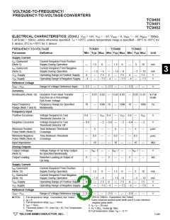
 TELCOM [ TELCOM SEMICONDUCTOR, INC ]