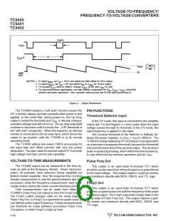
VOLTAGE-TO-FREQUENCY/
FREQUENCY-TO-VOLTAGECONVERTERS
1
2
3
4
5
6
7
8
TC9400
TC9401
TC9402
+5V
14
+
+
V
V
V
DD
*
f
OUT/2
10
9
TC9400A
TC9401A
TC9402A
Ϭ2
OUTPUT
COMMON
*
THRESHOLD
DETECT
*
f
SEE
FIGURE
6
8
11
3 µsec
DELAY
OUT
f
IN
* OPTIONAL
IF BUFFER
IS NEEDED
THRESHOLD
DETECTOR
V
REF
OUT
5
3
SEE
EQUATION,
PAGE 12
C
56 pF
REF
12pF
I
IN
OFFSET
ADJUST
R
1 MΩ
C
INT
INT
60pF
+
+5V
1000pF
AMP
OUT 12
–
OP
V
100kΩ
O
AMP
ZERO ADJUST
2
+
2 kΩ
2.2kΩ
I
V
V
7
BIAS
SS
REF
GND
6
1
4
10 kΩ
V
REF
(TYPICALLY –5V)
–5V
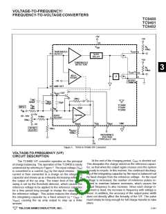
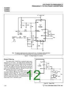
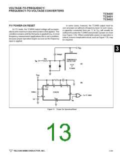
Figure 7. DC — 10 kHz F/V Converter
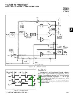
Input Buffer
5.0µsec
MIN
0.5µsec
fOUT and fOUT/2 are not used in the F/V mode. However,
these outputs may be useful for some applications, such as
a buffer to feed additional circuitry. Then, fOUT will follow the
input frequency waveform, except that fOUT will go high
3µsec after fIN goes high; fOUT/2 will be squarewave with a
MIN
INPUT
frequency of one-half fOUT
If these outputs are not used, pins 8, 9 and 10 should be
connected to ground.
.
f
OUT
DELAY = 3µsec
f
/2
OUT
Figure 8 . F/V Digital Outputs
TELCOM SEMICONDUCTOR, INC.
3-297

 TELCOM [ TELCOM SEMICONDUCTOR, INC ]