VOLTAGE-TO-FREQUENCY/
FREQUENCY-TO-VOLTAGE CONVERTERS
TC9400
TC9401
TC9402
Input Voltage Levels
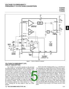
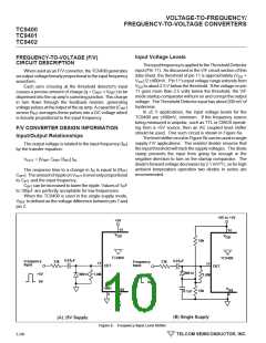
FREQUENCY-TO-VOLTAGE (F/V)
CIRCUIT DESCRIPTION
TheinputfrequencyisappliedtotheThresholdDetector
input (Pin 11). As discussed in the V/F circuit section of this
data sheet, the threshold of pin 11 is approximately (VDD
VSS) /2 ±400mV. Pin 11's input voltage range extends from
VDD to about 2.5 V below the threshold. If the voltage on pin
11 goes more than 2.5 volts below the threshold, the V/F
mode startup comparator will turn on and corrupt the output
voltage. The Threshold Detector input has about 200 mV of
hysteresis.
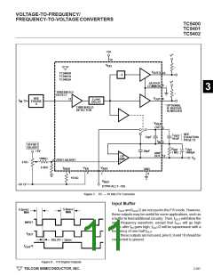
When used as an F/V converter, the TC9400 generates
anoutputvoltagelinearlyproportionaltotheinputfrequency
waveform.
Each zero crossing at the threshold detector's input
causes a precise amount of charge (q = CREF × VREF) to be
dispensed into the op amp's summing junction. This charge
in turn flows through the feedback resistor, generating
+
voltagepulsesattheoutputoftheopamp.Acapacitor(CINT
)
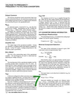
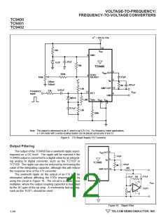
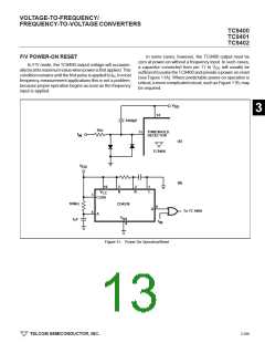
In ±5 V applications, the input voltage levels for the
TC9400 are ±400mV, minimum. If the frequency source
being measured is unipolar, such as TTL or CMOS operat-
ing from a +5V source, then an AC coupled level shifter
should be used. One such circuit is shown in Figure 6a.
ThelevelshiftercircuitinFigure6bcanbeusedinsingle
supply F/V applications. The resistor divider ensures that
the input threshold will track the supply voltages. The diode
clamp prevents the input from going far enough in the
negative direction to turn on the startup comparator. The
diode's forward voltage decreases by 2.1 mV/°C, so for high
ambient temperature operation two diodes in series are
recommended.
across RINT averages these pulses into a DC voltage which
is linearly proportional to the input frequency.
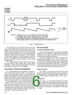
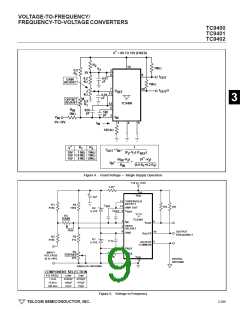
F/V CONVERTER DESIGN INFORMATION
Input/Output Relationships
The output voltage is related to the input frequency (fIN)
by the transfer equation:
VOUT = [VREF CREF RINT] fIN.
The response time to a change in fIN is equal to (RINT
CINT). TheamountofrippleonVOUT isinverselyproportional
to CINT and the input frequency.
CINT can be increased to lower the ripple. Values of 1µF
to 100µF are perfectly acceptable for low frequencies.
When the TC9400 is used in the single-supply mode,
VREF is defined as the voltage difference between pin 7 and
pin 2.
+8V to +5V
14
+5V
14
V
V
DD
DD
10k
TC9400
TC9400
0.01µF
0.01µF
Frequency
Input
33k
33k
Frequency
Input
11
11
DET
DET
IN914
+5V
0V
IN914 1.0M
+5V
0V
1.0M
GND
6
V
SS
4
V
SS
10k
0.1µF
4
–5V
(B) Single Supply
(A) ±5V Supply
Figure 6. Frequency Input Level Shifter
3-296
TELCOM SEMICONDUCTOR, INC.

 TELCOM [ TELCOM SEMICONDUCTOR, INC ]