VOLTAGE-TO-FREQUENCY/
FREQUENCY-TO-VOLTAGECONVERTERS
1
2
3
4
5
6
7
8
TC9400
TC9401
TC9402
+5V
14
+
5V
V
R
10kΩ
L
DD
f
THRESHOLD
DETECT
OUT 8
11
3µsec
DELAY
+
5V
THRESHOLD
DETECTOR
R
L
10kΩ
f
/2
OUT
10
9
SELF-
START
÷2
OUTPUT
COMMON
–3V
12 AMP OUT
V
OUT
REF
5
20kΩ
C
INT
C
REF
820pF
12pF
180pF
TC9400
TC9401
TC9402
R
1MΩ
IN
INPUT
60pF
I
IN
3
V
–
IN
+5V
OpAmp
+
ZERO
ADJUST
0V –10V
50kΩ
510kΩ
2
V
V
7
I
GND
6
SS
REF
BIAS
–5V
1
4
OFFSET
ADJUST
10kΩ
R
BIAS
100kΩ
REFERENCE
VOLTAGE
(TYPICALLY –5V)
–5V
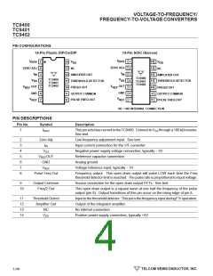
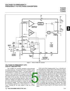
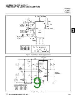
Figure 1. 10 Hz to 10 kHz V/F Converter
VOLTAGE-TO-FREQUENCY (V/F)
CIRCUIT DESCRIPTION
At the end of the charging period, CREF is shorted out.
This dissipates the charge stored on the reference capaci-
tor, so that when the output again crosses zero the system
is ready to recycle. In this manner, the continued discharg-
ing of the integrating capacitor by the input is balanced out
by fixed charges from the reference voltage. As the input
voltage is increased, the number of reference pulses re-
quired to maintain balance increases, which causes the
output frequency to also increase. Since each charge in-
crement is fixed, the increase in frequency with voltage is
linear. In addition, the accuracy of the output pulse width
does not directly affect the linearity of the V/F. The pulse
must simply be long enough for full charge transfer to take
place.
The TC9400 V/F converter operates on the principal
of charge balancing. The operation of the TC9400 is easily
understood by referring to Figure 1. The input voltage (VIN)
is converted to a current (IIN) by the input resistor. This
current is then converted to a charge on the integrating
capacitor and shows up as a linearly decreasing voltage at
the output of the op amp. The lower limit of the output
swing is set by the threshold detector, which causes the
reference voltage to be applied to the reference capacitor
for a time period long enough to charge the capacitor to
the reference voltage. This action reduces the charge on
the integrating capacitor by a fixed amount (q = CREF
×
VREF), causing the op amp output to step up a finite
amount.
TELCOM SEMICONDUCTOR, INC.
3-291

 TELCOM [ TELCOM SEMICONDUCTOR, INC ]