VOLTAGE-TO-FREQUENCY/
FREQUENCY-TO-VOLTAGECONVERTERS
TC9400
TC9401
TC9402
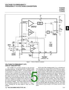
CREF
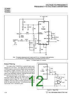
Improved Single Supply V/F Converter
Operation
Theexactvalueisnotcriticalandmaybeusedtotrimthe
full-scalefrequency(see"Input/OutputRelationships").Glass
film or air trimmer capacitors are recommended because of
their stability and low leakage. Locate as close as possible
to pins 5 and 3.
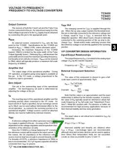
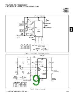
A TC9400 which operates from a single 12 to 15V
variablepowersourceisshowninFigure5. Thiscircuituses
twoZenerdiodestosetstablebiasinglevelsfortheTC9400.
The Zener diodes also provide the reference voltage, so the
outputimpedanceandtemperaturecoefficientoftheZeners
will directly affect power supply rejection and temperature
performance.
Full scale adjustment is accomplished by trimming the
input current. Trimming the reference voltage is not recom-
mended for high accuracy applications unless an op amp is
used as a buffer, because the TC9400 requires a low
impedance reference (see the VREF pin description section
for more information).
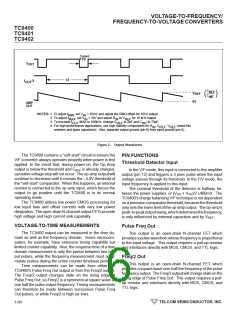
VDD, VSS
Power supplies of ±5V are recommended. For high-
accuracy requirements, 0.05% line and load regulation and
0.1µF disc decoupling capacitors located near the pins are
recommended.
Adjustment Procedure
Figure 1 shows a circuit for trimming the zero location.
The circuit of Figure 5 will directly interface with CMOS
logic operating at 12V to 15V. TTL or 5V CMOS logic can be
accommodated by connecting the output pullup resistors to
the +5V supply. An optoisolator can also be used if an
isolated output is required.
Full scale may be trimmed by adjusting RIN, VREF, or CREF
Recommended procedure for a 10kHz full-scale frequency
is as follows:
.
(1) Set VIN to 10 mV and trim the zero adjust circuit to
obtain a 10Hz output frequency.
(2) Set VIN to 10V and trim either RIN, VREF, or CREF to
obtain a 10kHz output frequency.
If adjustments are performed in this order, there should be
no interaction and they should not have to be repeated.
500
V
V
R
V
= +5V
= – 5V
= 1MΩ
= +10V
DD
SS
IN
400
300
200
100
IN
T
= +25°C
A
1 kHz
100kHz
–2
–3
–4
–5
–6
–7
0
–1
V
(V)
REF
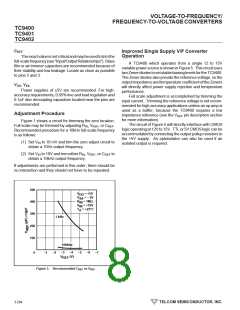
Figure 3. Recommended CREF vs VREF
3-294
TELCOM SEMICONDUCTOR, INC.

 TELCOM [ TELCOM SEMICONDUCTOR, INC ]