VOLTAGE-TO-FREQUENCY/
FREQUENCY-TO-VOLTAGECONVERTERS
TC9400
TC9401
TC9402
*Static-sensitive device. Unused devices must be stored in conductive
material. Protect devices from static discharge and static fields. Stresses
above those listed under Absolute Maximum Ratings may cause perma-
nent damage to the device. These are stress ratings only and functional
operation of the device at these or any other conditions above those
indicated in the operational sections of the specifications is not implied.
Exposure to Absolute Maximum Rating Conditions for extended periods
may affect device reliability.
ABSOLUTE MAXIMUM RATINGS*
VDD – VSS ................................................................. +18V
IIN ...........................................................................10mA
VOUT Max –VOUT Common..........................................23V
VREF – VSS ..............................................................– 1.5V
Storage Temperature Range ................ – 65°C to +150°C
Operating Temperature Range
C Device ................................................ 0°C to +70°C
E Device ........................................... – 40°C to +85°C
Package Dissipation (TA ≤ 70°C)
8-Pin CerDIP ..................................................800mW
8-Pin Plastic DIP.............................................730mW
8-Pin SOIC .....................................................470mW
Lead Temperature (Soldering, 10 sec) ................. +300°C
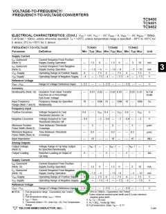
ELECTRICAL CHARACTERISTICS: VDD = +5V, VSS = – 5V, VGND = 0V, VREF = – 5V, RBIAS = 100kΩ,
Full Scale = 10kHz, unless otherwise specified. TA = +25°C, unless temperature range is specified (– 40°C to +85°C
for E device, 0°C to +70°C for C device).
VOLTAGE-TO-FREQUENCY
TC9401
TC9400
TC9402
Parameter
Definition
Min Typ Max Min Typ Max Min Typ Max
Unit
Accuracy
Linearity 10 kHz
Output Deviation From Straight
Line Between Normalized Zero
and Full-Scale Input
—
—
0.004 0.01
0.04 0.08
± 25 ± 40
—
—
0.01 0.05
0.1 0.25
—
—
0.05 0.25
% Full
Scale
Linearity 100 kHz
Output Deviation From Straight
Line Between Normalized Zero
Reading and Full-Scale Input
0.25
0.5
% Full
Scale
Gain Temperature
Drift (Note 1)
Variation in Gain A Due to
Temperature Change
—
—
—
—
—
—
—
—
± 25 ± 40 — ± 50 ± 100 ppm/°C
Full Scale
Gain Variance
Variation From Ideal Accuracy
± 10
–
± 10
—
— ± 10
–
% of
Nominal
Zero Offset (Note 2)
Correction at Zero Adjust for Zero
Output When Input is Zero
± 10 ± 50
± 25 ± 50
± 10 ± 50 — ± 20 ± 100
mV
Zero Temperature
Drift (Note 1)
Variation in Zero Offset Due to
Temperature Change
± 25 ± 50
—
± 50 ± 100 µV/°C
Analog Input
IIN Full Scale
Full-Scale Analog Input Current to
Achieve Specified Accuracy
—
10
—
—
10
—
10
—
µA
IIN Overrange
Overrange Current
—
—
—
2
50
—
—
—
—
2
50
—
—
—
—
2
50
—
µA
Response Time
Settling Time to 0.1% Full Scale
Cycle
Digital Section
VSAT @ IOL = 10mA
Logic "0" Output Voltage (Note 3)
—
—
0.2
—
0.4
18
—
—
0.2 0.4
—
—
0.2
—
0.4
18
V
V
VOUT Max – VOUT
Common (Note 4)
Voltage Range Between Output
and Common
—
18
Pulse Frequency
Output Width
—
3
—
—
3
—
—
3
—
µsec
3-288
TELCOM SEMICONDUCTOR, INC.

 TELCOM [ TELCOM SEMICONDUCTOR, INC ]