Document Number: PS-MPU-6500A-01
Revision: 1.1
Release Date: 03/05/2014
MPU-6500 Product Specification
4
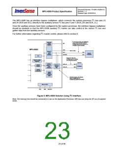
Applications Information
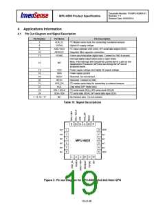
4.1 Pin Out Diagram and Signal Description
Pin Number
Pin Name
AUX_CL
VDDIO
Pin Description
I2C Master serial clock, for connecting to external sensors
7
8
Digital I/O supply voltage
9
AD0 / SDO
REGOUT
FSYNC
I2C Slave Address LSB (AD0); SPI serial data output (SDO)
Regulator filter capacitor connection
10
11
Frame synchronization digital input. Connect to GND if unused.
Interrupt digital output (totem pole or open-drain)
Note: The Interrupt line should be connected to a pin on the
Application Processor (AP) that can bring the AP out of
suspend mode.
12
INT
13
VDD
GND
Power supply voltage and Digital I/O supply voltage
Power supply ground
18
19
RESV
Reserved. Do not connect.
20
RESV
Reserved. Connect to GND.
I2C master serial data, for connecting to external sensors
21
AUX_DA
nCS
22
Chip select (SPI mode only)
23
24
SCL / SCLK
SDA / SDI
NC
I2C serial clock (SCL); SPI serial clock (SCLK)
I2C serial data (SDA); SPI serial data input (SDI)
No Connect pins. Do not connect.
1 – 6, 14 - 17
Table 10: Signal Descriptions
GND
NC
1
2
3
4
5
6
18
17
16
15
14
NC
NC
NC
NC
NC
NC
NC
NC
NC
MPU-6500
13 VDD
Figure 3: Pin out Diagram for MPU-6500 3.0x3.0x0.9mm QFN
19 of 40

 TDK [ TDK ELECTRONICS ]