Document Number: PS-MPU-6500A-01
Revision: 1.1
Release Date: 03/05/2014
MPU-6500 Product Specification
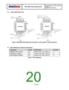
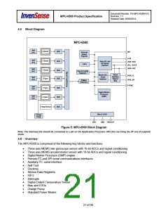
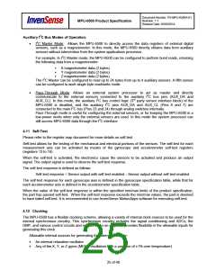
4.4 Block Diagram
MPU-6500
Self
test
X Accel
ADC
ADC
INT
Interrupt
Status
Register
nCS
Self
test
Y Accel
Slave I2C and
SPI Serial
Interface
AD0 / SDO
SCL / SCLK
SDA / SDI
FIFO
Self
test
Z Accel
X Gyro
ADC
ADC
User & Config
Registers
Serial
Interface
Bypass
Master I2C
Serial
Interface
AUX_CL
Self
test
AUX_DA
Mux
Sensor
Registers
FSYNC
Self
test
Y Gyro
Z Gyro
ADC
ADC
Digital Motion
Processor
(DMP)
Self
test
Temp Sensor
ADC
Bias & LDOs
Charge
Pump
VDD
GND
REGOUT
Figure 5: MPU-6500 Block Diagram
Note: The Interrupt line should be connected to a pin on the Application Processor (AP) that can bring the AP out of suspend
mode.
4.5 Overview
The MPU-6500 is comprised of the following key blocks and functions:
•
•
•
•
•
•
•
•
•
•
•
•
•
•
Three-axis MEMS rate gyroscope sensor with 16-bit ADCs and signal conditioning
Three-axis MEMS accelerometer sensor with 16-bit ADCs and signal conditioning
Digital Motion Processor (DMP) engine
Primary I2C and SPI serial communications interfaces
Auxiliary I2C serial interface
Self-Test
Clocking
Sensor Data Registers
FIFO
Interrupts
Digital-Output Temperature Sensor
Bias and LDOs
Charge Pump
Standard Power Modes
21 of 40

 TDK [ TDK ELECTRONICS ]