Document Number: PS-MPU-6500A-01
Revision: 1.1
Release Date: 03/05/2014
MPU-6500 Product Specification
4.6 Three-Axis MEMS Gyroscope with 16-bit ADCs and Signal Conditioning
The MPU-6500 consists of three independent vibratory MEMS rate gyroscopes, which detect rotation about
the X-, Y-, and Z- Axes. When the gyros are rotated about any of the sense axes, the Coriolis Effect causes
a vibration that is detected by a capacitive pickoff. The resulting signal is amplified, demodulated, and filtered
to produce a voltage that is proportional to the angular rate. This voltage is digitized using individual on-chip
16-bit Analog-to-Digital Converters (ADCs) to sample each axis. The full-scale range of the gyro sensors
may be digitally programmed to ±250, ±500, ±1000, or ±2000 degrees per second (dps). The ADC sample
rate is programmable from 8,000 samples per second, down to 3.9 samples per second, and user-selectable
low-pass filters enable a wide range of cut-off frequencies.
4.7 Three-Axis MEMS Accelerometer with 16-bit ADCs and Signal Conditioning
The MPU-6500’s 3-Axis accelerometer uses separate proof masses for each axis. Acceleration along a
particular axis induces displacement on the corresponding proof mass, and capacitive sensors detect the
displacement differentially. The MPU-6500’s architecture reduces the accelerometers’ susceptibility to
fabrication variations as well as to thermal drift. When the device is placed on a flat surface, it will measure
0g on the X- and Y-axes and +1g on the Z-axis. The accelerometers’ scale factor is calibrated at the factory
and is nominally independent of supply voltage. Each sensor has a dedicated sigma-delta ADC for providing
digital outputs. The full scale range of the digital output can be adjusted to ±2g, ±4g, ±8g, or ±16g.
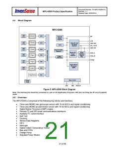
4.8 Digital Motion Processor
The embedded Digital Motion Processor (DMP) within the MPU-6500 offloads computation of motion
processing algorithms from the host processor. The DMP acquires data from accelerometers, gyroscopes,
and additional 3rd party sensors such as magnetometers, and processes the data. The resulting data can be
read from the FIFO. The DMP has access to one of the MPU’s external pins, which can be used for
generating interrupts.
The purpose of the DMP is to offload both timing requirements and processing power from the host
processor. Typically, motion processing algorithms should be run at a high rate, often around 200Hz, in order
to provide accurate results with low latency. This is required even if the application updates at a much lower
rate; for example, a low power user interface may update as slowly as 5Hz, but the motion processing should
still run at 200Hz. The DMP can be used to minimize power, simplify timing, simplify the software
architecture, and save valuable MIPS on the host processor for use in applications.
The DMP supports the following functionality:
•
Low Power Quaternion (3-Axis Gyroscope)
•
•
Screen Orientation (A low-power implementation of Android’s screen rotation algorithm)
Pedometer (InvenSense implementation)
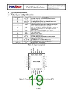
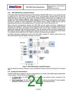
4.9 Primary I2C and SPI Serial Communications Interfaces
The MPU-6500 communicates to a system processor using either a SPI or an I2C serial interface. The MPU-
6500 always acts as a slave when communicating to the system processor. The LSB of the of the I2C slave
address is set by pin 9 (AD0).
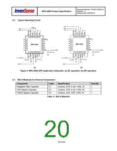
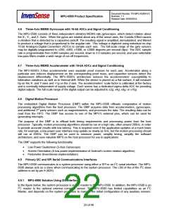
4.9.1 MPU-6500 Solution Using I2C Interface
In the figure below, the system processor is an I2C master to the MPU-6500. In addition, the MPU-6500 is an
I2C master to the optional external compass sensor. The MPU-6500 has limited capabilities as an I2C
Master, and depends on the system processor to manage the initial configuration of any auxiliary sensors.
22 of 40

 TDK [ TDK ELECTRONICS ]