Document Number: PS-MPU-6500A-01
Revision: 1.1
Release Date: 03/05/2014
MPU-6500 Product Specification
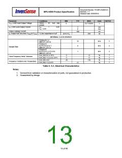
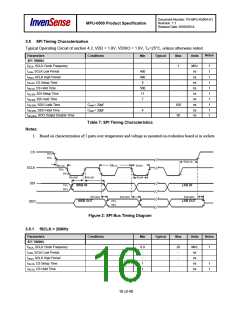
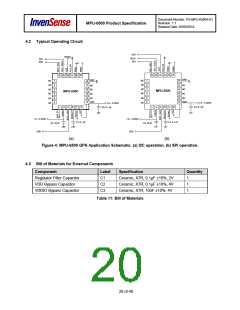
3.5 SPI Timing Characterization
Typical Operating Circuit of section 4.2, VDD = 1.8V, VDDIO = 1.8V, TA=25°C, unless otherwise noted.
Notes
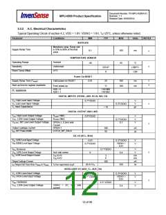
Parameters
Conditions
Min
Typical
Max
Units
SPI TIMING
fSCLK, SCLK Clock Frequency
1
MHz
ns
ns
ns
ns
ns
ns
ns
ns
ns
1
1
1
1
1
1
1
1
1
1
tLOW, SCLK Low Period
tHIGH, SCLK High Period
tSU.CS, CS Setup Time
tHD.CS, CS Hold Time
400
400
8
500
11
7
tSU.SDI, SDI Setup Time
tHD.SDI, SDI Hold Time
tVD.SDO, SDO Valid Time
tHD.SDO, SDO Hold Time
tDIS.SDO, SDO Output Disable Time
Cload = 20pF
Cload = 20pF
100
50
4
Table 7: SPI Timing Characteristics
Notes:
1. Based on characterization of 5 parts over temperature and voltage as mounted on evaluation board or in sockets
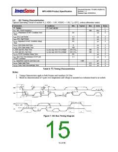
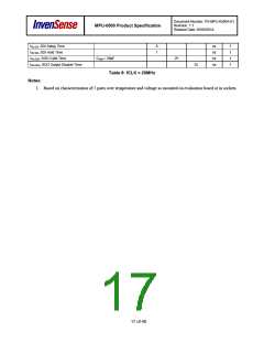
Figure 2: SPI Bus Timing Diagram
3.5.1 fSCLK = 20MHz
Parameters
Conditions
Min
Typical
Max
Units
Notes
SPI TIMING
fSCLK, SCLK Clock Frequency
tLOW, SCLK Low Period
tHIGH, SCLK High Period
tSU.CS, CS Setup Time
tHD.CS, CS Hold Time
0.9
-
20
-
MHz
ns
1
-
-
ns
1
ns
1
1
1
ns
16 of 40

 TDK [ TDK ELECTRONICS ]