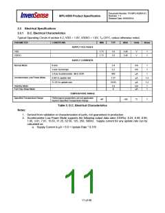
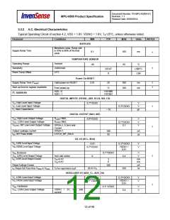
Document Number: PS-MPU-6500A-01
Revision: 1.1
Release Date: 03/05/2014
MPU-6500 Product Specification
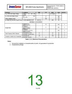
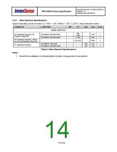
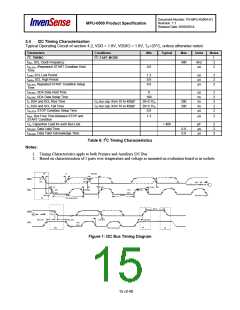
3.4
I2C Timing Characterization
Typical Operating Circuit of section 4.2, VDD = 1.8V, VDDIO = 1.8V, TA=25°C, unless otherwise noted.
Parameters
Conditions
I2C FAST-MODE
Min
Typical
Max
Units
Notes
I2C TIMING
1
2
2
fSCL, SCL Clock Frequency
400
kHz
µs
tHD.STA, (Repeated) START Condition Hold
Time
0.6
tLOW, SCL Low Period
tHIGH, SCL High Period
1.3
0.6
0.6
µs
µs
µs
2
2
2
tSU.STA, Repeated START Condition Setup
Time
tHD.DAT, SDA Data Hold Time
tSU.DAT, SDA Data Setup Time
tr, SDA and SCL Rise Time
tf, SDA and SCL Fall Time
0
µs
ns
ns
ns
µs
2
2
2
2
2
100
Cb bus cap. from 10 to 400pF
Cb bus cap. from 10 to 400pF
20+0.1Cb
20+0.1Cb
0.6
300
300
tSU.STO, STOP Condition Setup Time
tBUF, Bus Free Time Between STOP and
START Condition
1.3
µs
2
Cb, Capacitive Load for each Bus Line
tVD.DAT, Data Valid Time
< 400
pF
µs
µs
2
2
2
0.9
0.9
tVD.ACK, Data Valid Acknowledge Time
Table 6: I2C Timing Characteristics
Notes:
1. Timing Characteristics apply to both Primary and Auxiliary I2C Bus
2. Based on characterization of 5 parts over temperature and voltage as mounted on evaluation board or in sockets
Figure 1: I2C Bus Timing Diagram
15 of 40

 TDK [ TDK ELECTRONICS ]