Document Number: PS-MPU-6500A-01
Revision: 1.1
Release Date: 03/05/2014
MPU-6500 Product Specification
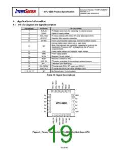
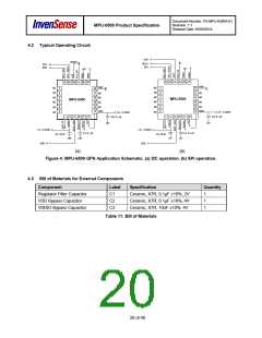
4.2 Typical Operating Circuit
nCS
VDDIO
SCLK
SDI
SCL
SDA
GND
18
GND
NC
1
2
3
4
5
6
NC
NC
1
2
3
4
5
6
18
NC
17
17
16
15
14
13
NC
NC
NC
NC
NC
NC
NC
16
15
14
13
NC
NC
MPU-6500
MPU-6500
NC
NC
NC
NC
NC
NC
NC
VDD
VDD
1.8 – 3.3VDC
C2, 0.1 µF
1.8 – 3.3VDC
C2, 0.1 µF
1.8 – 3.3VDC
1.8 – 3.3VDC
C1, 0.1 µF
C1, 0.1 µF
C3, 10 nF
C3, 10 nF
AD0
SD0
(a)
(b)
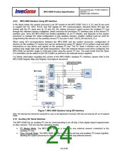
Figure 4: MPU-6500 QFN Application Schematic. (a) I2C operation, (b) SPI operation.
4.3 Bill of Materials for External Components
Component
Label
C1
Specification
Quantity
Regulator Filter Capacitor
VDD Bypass Capacitor
VDDIO Bypass Capacitor
Ceramic, X7R, 0.1µF ±10%, 2V
Ceramic, X7R, 0.1µF ±10%, 4V
Ceramic, X7R, 10nF ±10%, 4V
1
1
1
C2
C3
Table 11: Bill of Materials
20 of 40

 TDK [ TDK ELECTRONICS ]