UPSD3212C, UPSD3212CV
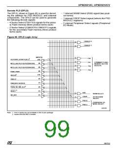
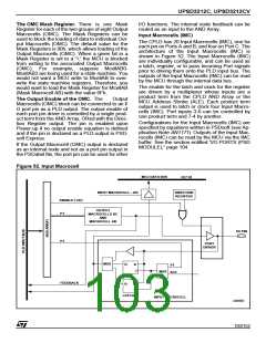
Decode PLD (DPLD)
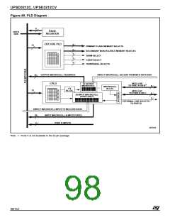
The DPLD, shown in Figure 49, is used for decod-
ing the address for PSD MODULE and external
components. The DPLD can be used to generate
the following decode signals:
– 1 internal SRAM Select (RS0) signal (two prod-
uct terms)
– 1 internal CSIOP Select signal (selects the PSD
MODULE registers)
– 4 Sector Select (FS0-FS3) signals for the prima-
ry Flash memory (three product terms each)
– 2 internal Peripheral Select signals (Peripheral
I/O Mode).
– 2 Sector Select (CSBOOT0-CSBOOT1) signals
for the secondary Flash memory (three product
terms each)
Figure 49. DPLD Logic Array
CSBOOT 0
CSBOOT 1
3
3
(INPUTS)
1
3
3
3
3
FS0
I/O PORTS (PORT A,B,C)
(20)
4 PRIMARY FLASH
MEMORY SECTOR
SELECTS
FS1
FS2
(8)
MCELLAB.FB [7:0] (FEEDBACKS)
MCELLBC.FB [7:0] (FEEDBACKS)
(8)
(8)
FS3
PGR0 -PGR7
2
(16)
(2)
[
]
A 15:0
[
]
PD 2:1
PDN (APD OUTPUT)
(1)
(4)
(1)
(1)
2
PSEN, RD, WR, ALE
2
RESET
RS0
2
1
SRAM SELECT
RD_BSY
CSIOP
PSEL0
PSEL1
I/O DECODER
SELECT
1
1
PERIPHERAL I/O
MODE SELECT
AI07436
Note: 1. Port A inputs are not available in the 52-pin package
2. Inputs from the MCU module
99/152

 STMICROELECTRONICS [ ST ]