UPSD3212C, UPSD3212CV
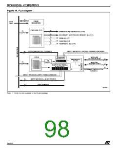
PLDS
The PLDs bring programmable logic functionality
to the uPSD. After specifying the logic for the
PLDs in PSDsoft Express, the logic is pro-
grammed into the device and available upon Pow-
er-up.
The PSD MODULE contains two PLDs: the De-
code PLD (DPLD), and the Complex PLD (CPLD).
The PLDs are briefly discussed in the next few
paragraphs, and in more detail in the section enti-
tled “Decode PLD (DPLD),” page 99, and the sec-
tion entitled “Complex PLD (CPLD),” page 100.
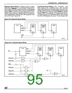
Figure 48 shows the configuration of the PLDs.
The DPLD performs address decoding for Select
signals for PSD MODULE components, such as
memory, registers, and I/O ports.
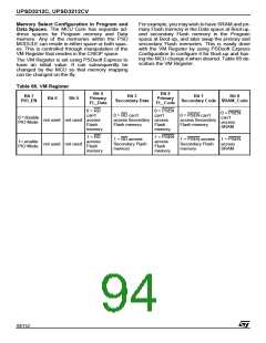
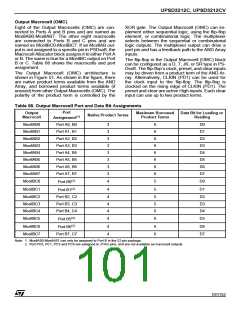
Table 67. DPLD and CPLD Inputs
Number
Input Source
Input Name
of
Signals
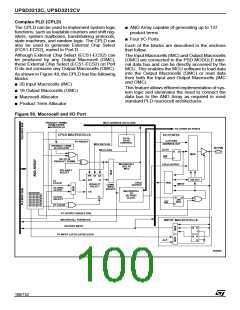
The CPLD can be used for logic functions, such as
loadable counters and shift registers, state ma-
chines, and encoding and decoding logic. These
logic functions can be constructed using the Out-
put Macrocells (OMC), Input Macrocells (IMC),
and the AND Array. The CPLD can also be used
to generate External Chip Select (ECS1-ECS2)
signals.
A15-A0
16
4
MCU Address Bus
PSEN, RD, WR,
ALE
MCU Control Signals
RESET
RST
PDN
1
1
Power-down
The AND Array is used to form product terms.
These product terms are specified using PSDsoft.
The PLD input signals consist of internal MCU sig-
nals and external inputs from the I/O ports. The in-
put signals are shown in Table 67.
Port A Input
PA7-PA0
8
8
4
1
Macrocells
Port B Input
Macrocells
PB7-PB0
The Turbo Bit in PSD MODULE
Port C Input
Macrocells
PC7, PC4-PC2
The PLDs can minimize power consumption by
switching off when inputs remain unchanged for
an extended time of about 70ns. Resetting the
Turbo Bit to '0' (Bit 3 of PMMR0) automatically
places the PLDs into standby if no inputs are
changing. Turning the Turbo Mode off increases
propagation delays while reducing power con-
sumption. See the section entitled “POWER MAN-
AGEMENT,” page 113, on how to set the Turbo
Bit.
Additionally, five bits are available in PMMR2 to
block MCU control signals from entering the PLDs.
This reduces power consumption and can be used
only when these MCU control signals are not used
in PLD logic equations.
PD2-PD1
2
8
Port D Inputs
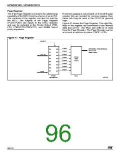
Page Register
PGR7-PGR0
Macrocell AB
Feedback
MCELLAB.FB7-
FB0
8
8
1
Macrocell BC
Feedback
MCELLBC.FB7-
FB0
Flash memory
Program Status Bit
Ready/Busy
Note: 1. These inputs are not available in the 52-pin package.
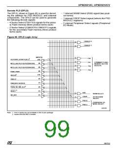
Each of the two PLDs has unique characteristics
suited for its applications. They are described in
the following sections.
97/152

 STMICROELECTRONICS [ ST ]