UPSD3212C, UPSD3212CV
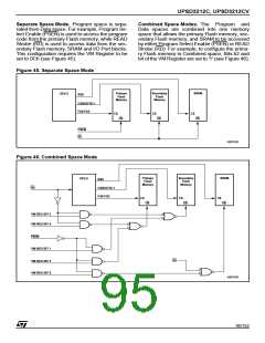
Separate Space Mode. Program space is sepa-
rated from Data space. For example, Program Se-
lect Enable (PSEN) is used to access the program
code from the primary Flash memory, while READ
Strobe (RD) is used to access data from the sec-
ondary Flash memory, SRAM and I/O Port blocks.
This configuration requires the VM Register to be
set to 0Ch (see Figure 45).
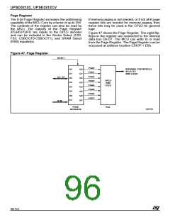
Combined Space Modes. The Program and
Data spaces are combined into one memory
space that allows the primary Flash memory, sec-
ondary Flash memory, and SRAM to be accessed
by either Program Select Enable (PSEN) or READ
Strobe (RD). For example, to configure the prima-
ry Flash memory in Combined space, Bits b2 and
b4 of the VM Register are set to '1' (see Figure 46).
Figure 45. Separate Space Mode
Primary
Flash
Secondary
Flash
SRAM
DPLD
RS0
Memory
Memory
CSBOOT0-1
FS0-FS3
CS
CS
OE
CS
OE
OE
PSEN
RD
AI07433
Figure 46. Combined Space Mode
Primary
Flash
Secondary
Flash
SRAM
DPLD
RS0
Memory
Memory
RD
CSBOOT0-1
FS0-FS3
CS
CS
OE
CS
OE
OE
VM REG BIT 3
VM REG BIT 4
PSEN
VM REG BIT 1
RD
VM REG BIT 2
VM REG BIT 0
AI07434
95/152

 STMICROELECTRONICS [ ST ]