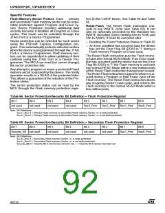
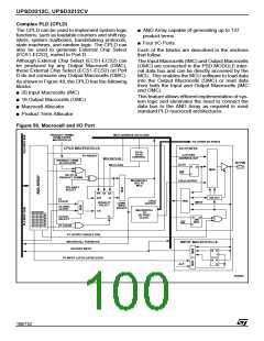
UPSD3212C, UPSD3212CV
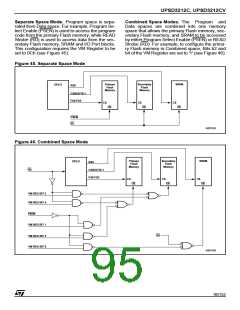
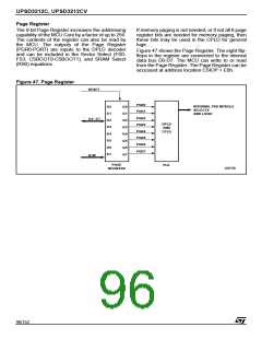
Page Register
The 8-bit Page Register increases the addressing
capability of the MCU Core by a factor of up to 256.
The contents of the register can also be read by
the MCU. The outputs of the Page Register
(PGR0-PGR7) are inputs to the DPLD decoder
and can be included in the Sector Select (FS0-
FS3, CSBOOT0-CSBOOT1), and SRAM Select
(RS0) equations.
If memory paging is not needed, or if not all 8 page
register bits are needed for memory paging, then
these bits may be used in the CPLD for general
logic.
Figure 47 shows the Page Register. The eight flip-
flops in the register are connected to the internal
data bus D0-D7. The MCU can write to or read
from the Page Register. The Page Register can be
accessed at address location CSIOP + E0h.
Figure 47. Page Register
RESET
PGR0
INTERNAL PSD MODULE
SELECTS
AND LOGIC
D0
D1
D2
D3
D4
D5
D6
D7
Q0
PGR1
Q1
Q2
Q3
Q4
Q5
Q6
Q7
PGR2
D0 - D7
DPLD
AND
CPLD
PGR3
PGR4
PGR5
PGR6
PGR7
R/W
PAGE
REGISTER
PLD
AI05799
96/152

 STMICROELECTRONICS [ ST ]