UPSD3212C, UPSD3212CV
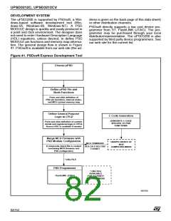
In-System Programming (ISP)
Using the JTAG signals on Port C, the entire PSD
MODULE device can be programmed or erased
without the use of the MCU. The primary Flash
memory can also be programmed in-system by
the MCU executing the programming algorithms
out of the secondary memory, or SRAM. The sec-
ondary memory can be programmed the same
way by executing out of the primary Flash memo-
ry. The PLD or other PSD MODULE Configuration
blocks can be programmed through the JTAG port
or a device programmer. Table 60 indicates which
programming methods can program different func-
tional blocks of the PSD MODULE.
Table 60. Methods of Programming Different Functional Blocks of the PSD MODULE
Functional Block
Primary Flash Memory
JTAG Programming Device Programmer
IAP
Yes
Yes
Yes
Yes
Yes
Yes
Yes
Yes
Yes
Yes
No
Secondary Flash Memory
PLD Array (DPLD and CPLD)
PSD MODULE Configuration
No
81/152

 STMICROELECTRONICS [ ST ]