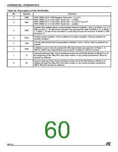
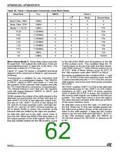
UPSD3212C, UPSD3212CV
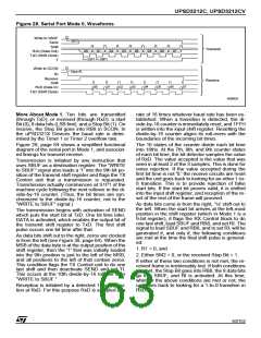
Figure 28. Serial Port Mode 0, Waveforms
Write to SBUF
S6P2
Send
Shift
Transmit
D0
S3P1
D1
S6P1
D2
D3
D4
D5
D6
D7
RxD (Data Out)
TxD (Shift Clock)
T
Write to SCON
Clear RI
RI
Receive
Shift
RxD (Data In)
TxD (Shift Clock)
Receive
D0
D1
D2
D3
D4
D5
D6
D7
AI06825
More About Mode 1. Ten bits are transmitted
(through TxD), or received (through RxD): a start
Bit (0), 8 data bits (LSB first). and a Stop Bit (1). On
receive, the Stop Bit goes into RB8 in SCON. In
the uPSD321X Devices the baud rate is deter-
mined by the Timer 1 or Timer 2 overflow rate.
rate of 16 times whatever baud rate has been es-
tablished. When a transition is detected, the di-
vide-by-16 counter is immediately reset, and 1FFH
is written into the input shift register. Resetting the
divide-by-16 counter aligns its roll-overs with the
boundaries of the incoming bit times.
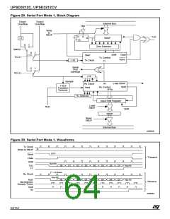
Figure 29, page 64 shows a simplified functional
diagram of the serial port in Mode 1, and associat-
ed timings for transmit receive.
The 16 states of the counter divide each bit time
into 16ths. At the 7th, 8th, and 9th counter states
of each bit time, the bit detector samples the value
of RxD. The value accepted is the value that was
seen in at least 2 of the 3 samples. This is done for
noise rejection. If the value accepted during the
first bit time is not '0,' the receive circuits are reset
and the unit goes back to looking for an-other 1-to-
0 transition. This is to provide rejection of false
start bits. If the start bit proves valid, it is shifted
into the input shift register, and reception of the re-
set of the rest of the frame will proceed.
As data bits come in from the right, '1s' shift out to
the left. When the start bit arrives at the left-most
position in the shift register (which in Mode 1 is a
9-bit register), it flags the RX Control block to do
one last shift, load SBUF and RB8, and set RI. The
signal to load SBUF and RB8, and to set RI, will be
generated if, and only if, the following conditions
are met at the time the final shift pulse is generat-
ed:
Transmission is initiated by any instruction that
uses SBUF as a destination register. The “WRITE
to SBUF” signal also loads a '1' into the 9th bit po-
sition of the transmit shift register and flags the TX
Control unit that a transmission is requested.
Transmission actually commences at S1P1 of the
machine cycle following the next rollover in the di-
vide-by-16 counter. (Thus, the bit times are syn-
chronized to the divide-by-16 counter, not to the
“WRITE to SBUF” signal.)
The transmission begins with activation of SEND
which puts the start bit at TxD. One bit time later,
DATA is activated, which enables the output bit of
the transmit shift register to TxD. The first shift
pulse occurs one bit time after that.
As data bits shift out to the right, zeros are clocked
in from the left (see Figure 30, page 64). When the
MSB of the data byte is at the output position of the
shift register, then the '1' that was initially loaded
into the 9th position is just to the left of the MSB,
and all positions to the left of that contain zeros.
This condition flags the TX Control unit to do one
last shift and then deactivate SEND and set TI.
This occurs at the 10th divide-by-16 rollover after
“WRITE to SBUF.”
1. R1 = 0, and
2. Either SM2 = 0, or the received Stop Bit = 1.
If either of these two conditions is not met, the re-
ceived frame is irretrievably lost. If both conditions
are met, the Stop Bit goes into RB8, the 8 data bits
go into SBUF, and RI is activated. At this time,
whether the above conditions are met or not, the
unit goes back to looking for a 1-to-0 transition in
RxD.
Reception is initiated by a detected 1-to-0 transi-
tion at RxD. For this purpose RxD is sampled at a
63/152

 STMICROELECTRONICS [ ST ]