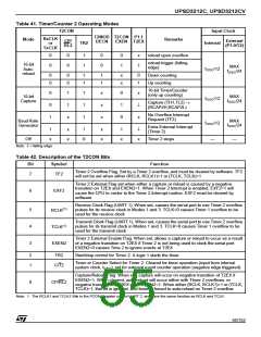
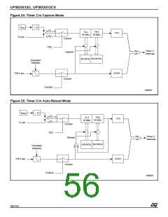
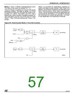
UPSD3212C, UPSD3212CV
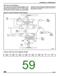
Serial Port Control Register
The serial port control and status register is the
Special Function Register SCON (SCON2 for the
second port), shown in Figure 27. This register
(see Tables 43 and 44) contains not only the mode
selection bits, but also the 9th data bit for transmit
and receive (TB8 and RB8), and the Serial Port In-
terrupt Bits (TI and RI).
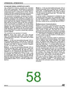
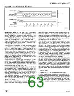
Figure 27. Serial Port Mode 0, Block Diagram
Internal Bus
Write
to
SBUF
RxD
D
S
P3.0 Alt
Output
Function
Q
SBUF
CL
Zero Detector
Shift
Start
Tx Control
T
Send
S6
Tx Clock
Serial
Port
Interrupt
Shift
Clock
TxD
Receive
Shift
6 5 4 3 2 1 0
R
P3.1 Alt
Output
Function
Rx Clock
Start
REN
R1
Rx Control
7
RxD
P3.0 Alt
Input
Function
Input Shift Register
Load
SBUF
Shift
SBUF
Read
SBUF
Internal Bus
AI06824
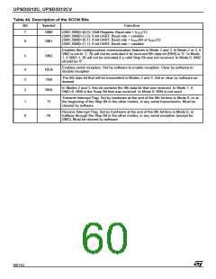
Table 43. Serial Port Control Register (SCON)
7
6
5
4
3
2
1
0
SM0
SM1
SM2
REN
TB8
RB8
TI
RI
59/152

 STMICROELECTRONICS [ ST ]