UPSD3212C, UPSD3212CV
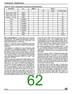
Table 45. Timer 1-Generated Commonly Used Baud Rates
f
Baud Rate
SMOD
Timer 1
OSC
C/T
X
X
0
Mode
Reload Value
Mode 0 Max: 1MHz
12MHz
12MHz
X
1
1
1
0
0
0
0
0
0
0
X
X
2
2
2
2
2
2
2
2
1
X
X
Mode 2 Max: 375K
Modes 1, 3: 62.5K
12MHz
FFh
FDh
FDh
FAh
F4h
E8h
1Dh
72h
FEEBh
19.2K
9.6K
4.8K
2.4K
1.2K
137.5
110
11.059MHz
11.059MHz
11.059MHz
11.059MHz
11.059MHz
11.059MHz
6MHz
0
0
0
0
0
0
0
110
12MHz
0
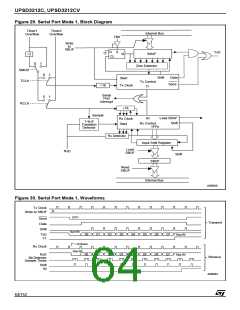
More About Mode 0. Serial data enters and exits
through RxD. TxD outputs the shift clock. 8 bits are
transmitted/received: 8 data bits (LSB first). The
to the left of the MSB, and all positions to the left
of that contain zeros. This condition flags the TX
Control block to do one last shift and then deacti-
vate SEND and set T1. Both of these actions occur
at S1P1. Both of these actions occur at S1P1 of
the 10th machine cycle after “WRITE to SBUF.”
Reception is initiated by the condition REN = 1 and
R1 = 0. At S6P2 of the next machine cycle, the RX
Control unit writes the bits 11111110 to the receive
shift register, and in the next clock phase activates
RECEIVE.
RECEIVE enables SHIFT CLOCK to the alternate
output function line of TxD. SHIFT CLOCK makes
transitions at S3P1 and S6P1 of every machine
cycle in which RECEIVE is active, the contents of
the receive shift register are shifted to the left one
position. The value that comes in from the right is
the value that was sampled at the RxD pin at S5P2
of the same machine cycle.
As data bits come in from the right, '1s' shift out to
the left. When the '0' that was initially loaded into
the right-most position arrives at the left-most po-
sition in the shift register, it flags the RX Control
block to do one last shift and load SBUF. At S1P1
of the 10th machine cycle after the WRITE to
SCON that cleared RI, RECEIVE is cleared as RI
is set.
baud rate is fixed at 1/12 the f
.
OSC
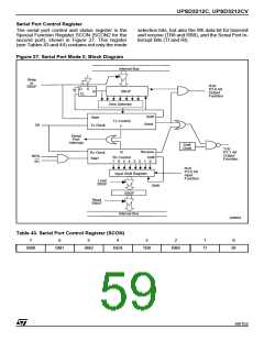
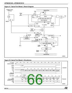
Figure 27, page 59 shows a simplified functional
diagram of the serial port in Mode 0, and associat-
ed timing.
Transmission is initiated by any instruction that
uses SBUF as a destination register. The “WRITE
to SBUF” signal at S6P2 also loads a '1' into the
9th position of the transmit shift register and tells
the TX Control block to commence a transmission.
The internal timing is such that one full machine
cycle will elapse between “WRITE to SBUF” and
activation of SEND.
SEND enables the output of the shift register to the
alternate out-put function line of RxD and also en-
able SHIFT CLOCK to the alternate output func-
tion line of TxD. SHIFT CLOCK is low during S3,
S4, and S5 of every machine cycle, and high dur-
ing S6, S1, and S2. At S6P2 of every machine cy-
cle in which SEND is active, the contents of the
transmit shift are shifted to the right one position.
As data bits shift out to the right, zeros come in
from the left. When the MSB of the data byte is at
the output position of the shift register, then the '1'
that was initially loaded into the 9th position, is just
62/152

 STMICROELECTRONICS [ ST ]