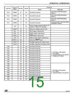
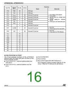
UPSD3212C, UPSD3212CV
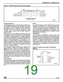
Figure 9. PSW (Program Status Word) Register
MSB
LSB
P
CY AC FO RS1 RS0 OV
Reset Value 00h
PSW
Carry Flag
Parity Flag
Auxillary Carry Flag
Bit not assigned
Overflow Flag
General Purpose Flag
Register Bank Select Flags
(to select Bank0-3)
AI06639
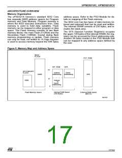
Program Memory
RAM
The program memory consists of two Flash mem-
ory: 64KByte Main Flash and 16KByte of Second-
ary Flash. The Flash memory can be mapped to
any address space as defined by the user in the
PSDsoft Tool. It can also be mapped to Data
memory space during Flash memory update or
programming.
Four register banks, each 8 registers wide, occupy
locations 0 through 31 in the lower RAM area.
Only one of these banks may be enabled at a time.
The next 16 bytes, locations 32 through 47, con-
tain 128 directly addressable bit locations. The
stack depth is only limited by the available internal
RAM space of 256 bytes.
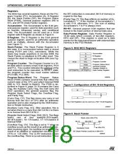
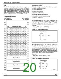
After reset, the CPU begins execution from loca-
tion 0000h. As shown in Figure 10, each interrupt
is assigned a fixed location in Program Memory.
The interrupt causes the CPU to jump to that loca-
tion, where it commences execution of the service
routine. External Interrupt 0, for example, is as-
signed to location 0003h. If External Interrupt 0 is
going to be used, its service routine must begin at
location 0003h. If the interrupt is not going to be
used, its service location is available as general
purpose Program Memory.
XRAM-PSD
The 2K bytes of XRAM-PSD resides in the PSD
Module and can be mapped to any address space
through the DPLD (Decoding PLD) as defined by
the user in PSDsoft Development tool. The XRAM-
PSD has a battery backup feature that allow the
data to be retained in the event of a power lost.
The battery is connected to the Port C PC2 pin.
This pin must be configured in PSDSoft to be bat-
tery back-up.
The interrupt service locations are spaced at 8-
byte intervals: 0003h for External Interrupt 0,
000Bh for Timer 0, 0013h for External Interrupt 1,
001Bh for Timer 1 and so forth. If an interrupt ser-
vice routine is short enough (as is often the case
in control applications), it can reside entirely within
that 8-byte interval (see Figure 10). Longer service
routines can use a jump instruction to skip over
subsequent interrupt locations, if other interrupts
are in use.
Figure 10. Interrupt Location of Program
Memory
008Bh
•
•
•
•
•
•
•
•
•
Interrupt
Location
0013h
8 Bytes
000Bh
0003h
Data memory
The internal data memory is divided into four phys-
ically separated blocks: 256 bytes of internal RAM,
128 bytes of Special Function Registers (SFRs)
areas and 2K bytes (XRAM-PSD) in the PSD Mod-
ule.
Reset
0000h
AI06640
19/152

 STMICROELECTRONICS [ ST ]