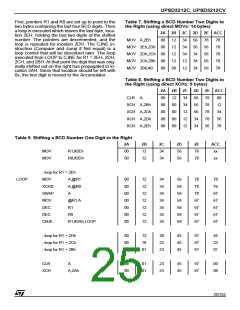
UPSD3212C, UPSD3212CV
(3) Register addressing. The register banks,
containing registers R0 through R7, can be ac-
cessed by certain instructions which carry a 3-bit
register specification within the opcode of the in-
struction. Instructions that access the registers
this way are code efficient, since this mode elimi-
nates an address byte. When the instruction is ex-
ecuted, one of four banks is selected at execution
time by the two bank select bits in the PSW.
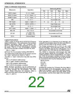
Arithmetic Instructions
The arithmetic instructions is listed in Table 4,
page 22. The table indicates the addressing
modes that can be used with each instruction to
access the <byte> operand. For example, the
ADD A, <byte> instruction can be written as:
ADD a, 7FH (direct addressing)
ADD A, @R0 (indirect addressing)
ADD a, R7 (register addressing)
ADD A, #127 (immediate constant)
Example:
mov PSW, #0001000B ; select Bank0
mov A, #30H
mov R1, A
Note: Any byte in the internal Data Memory space
can be incremented without going through the Ac-
cumulator.
One of the INC instructions operates on the 16-bit
Data Pointer. The Data Pointer is used to generate
16-bit addresses for external memory, so being
able to increment it in one 16-bit operations is
(4) Register-specific addressing. Some
in-
structions are specific to a certain register. For ex-
ample, some instructions always operate on the
Accumulator, or Data Pointer, etc., so no address
byte is needed to point it. The opcode itself does
that.
a useful feature.
The MUL AB instruction multiplies the Accumula-
tor by the data in the B register and puts the 16-bit
product into the concatenated B and Accumulator
registers.
The DIV AB instruction divides the Accumulator by
the data in the B register and leaves the 8-bit quo-
tient in the Accumulator, and the 8-bit remainder in
the B register.
In shift operations, dividing a number by 2n shifts
its “n” bits to the right. Using DIV AB to perform the
division completes the shift in 4?s and leaves the
B register holding the bits that were shifted out.
The DAA instruction is for BCD arithmetic opera-
tions. In BCD arithmetic, ADD and ADDC instruc-
tions should always be followed by a DAA
operation, to ensure that the result is also in BCD.
Note: DAA will not convert a binary number to
BCD. The DAA operation produces a meaningful
result only as the second step in the addition of
two BCD bytes.
(5) Immediate constants addressing. The val-
ue of a constant can follow the opcode in Program
memory.
Example:
mov A, #10H.
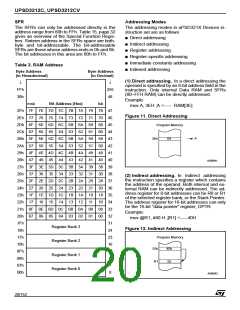
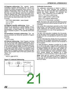
(6) Indexed addressing. Only Program memory
can be accessed with indexed addressing, and it
can only be read. This addressing mode is intend-
ed for reading look-up tables in Program memory.
A 16-bit base register (either DPTR or PC) points
to the base of the table, and the Accumulator is set
up with the table entry number. The address of the
table entry in Program memory is formed by add-
ing the Accumulator data to the base pointer (see
Figure 13).
Example:
movc A, @A+DPTR
Figure 13. Indexed Addressing
ACC
3Ah
DPTR
1E73h
Program Memory
3Eh
AI06643
21/152

 STMICROELECTRONICS [ ST ]