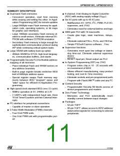
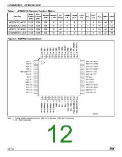
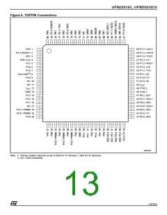
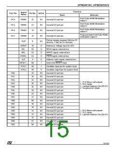
UPSD3212C, UPSD3212CV
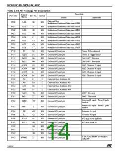
Function
Signal
Name
Port Pin
Pin No. In/Out
Basic
General I/O port pin
Alternate
8-bit Pulse Width Modulation
output 1
P4.4
P4.5
P4.6
P4.7
PWM1
PWM2
PWM3
PWM4
PUP
25
23
19
18
8
I/O
I/O
I/O
I/O
I/O
8-bit Pulse Width Modulation
output 2
General I/O port pin
General I/O port pin
General I/O port pin
8-bit Pulse Width Modulation
output 3
Programmable 8-bit Pulse Width
modulation output 4
Pull-up resistor required (2kΩ for 3V
devices, 7.5kΩ for 5V devices)
AVREF
RD_
70
65
62
63
4
O
O
Reference Voltage input for ADC
READ signal, external bus
WRITE signal, external bus
PSEN signal, external bus
Address Latch signal, external bus
Active low RESET input
Oscillator input pin for system clock
Oscillator output pin for system clock
General I/O port pin
WR_
O
PSEN_
ALE
O
O
RESET_
XTAL1
XTAL2
68
48
49
35
34
32
28
26
24
22
21
80
78
76
74
73
72
67
66
I
I
O
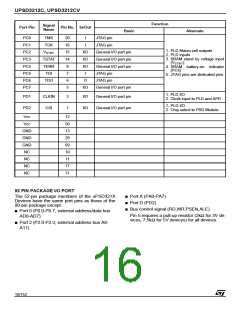
PA0
PA1
PA2
PA3
PA4
PA5
PA6
PA7
PB0
PB1
PB2
PB3
PB4
PB5
PB6
PB7
I/O
I/O
I/O
I/O
I/O
I/O
I/O
I/O
I/O
I/O
I/O
I/O
I/O
I/O
I/O
I/O
General I/O port pin
General I/O port pin
1. PLD Macro-cell outputs
2. PLD inputs
3. Latched Address Out (A0-A7)
4. Peripheral I/O Mode
General I/O port pin
General I/O port pin
General I/O port pin
General I/O port pin
General I/O port pin
General I/O port pin
General I/O port pin
General I/O port pin
1. PLD Macro-cell outputs
2. PLD inputs
3. Latched Address Out (A0-A7)
General I/O port pin
General I/O port pin
General I/O port pin
General I/O port pin
General I/O port pin
15/152

 STMICROELECTRONICS [ ST ]