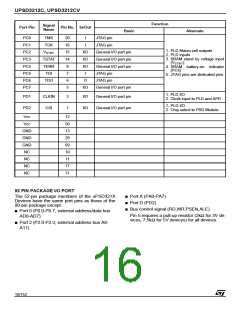
UPSD3212C, UPSD3212CV
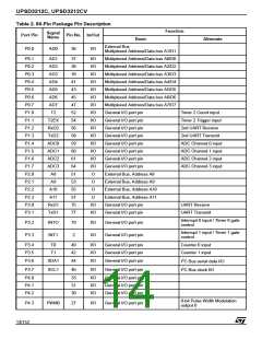
Function
Signal
Name
Port Pin
Pin No. In/Out
Basic
Alternate
PC0
PC1
PC2
PC3
PC4
PC5
PC6
PC7
TMS
TCK
20
16
15
14
9
I
JTAG pin
JTAG pin
I
1. PLD Macro-cell outputs
2. PLD inputs
V
STBY
I/O
I/O
I/O
I
General I/O port pin
General I/O port pin
General I/O port pin
JTAG pin
3. SRAM stand by voltage input
TSTAT
TERR
TDI
(V
)
STBY
4. SRAM battery-on indicator
(PC4)
7
5. JTAG pins are dedicated pins
TDO
6
O
JTAG pin
5
I/O
General I/O port pin
1. PLD I/O
2. Clock input to PLD and APD
PD1
PD2
CLKIN
CSI
3
1
I/O
I/O
General I/O port pin
General I/O port pin
1. PLD I/O
2. Chip select to PSD Module
Vcc
Vcc
GND
GND
GND
NC
12
50
13
29
69
10
11
17
71
NC
NC
NC
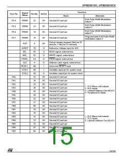
52 PIN PACKAGE I/O PORT
The 52-pin package members of the uPSD321X
Devices have the same port pins as those of the
80-pin package except:
■ Port A (PA0-PA7)
■ Port D (PD2)
■ Bus control signal (RD,WR,PSEN,ALE)
■ Port 0 (P0.0-P0.7, external address/data bus
Pin 5 requires a pull-up resistor (2kΩ for 3V de-
vices, 7.5kΩ for 5V devices) for all devices.
AD0-AD7)
■ Port 2 (P2.0-P2.3, external address bus A8-
A11)
16/152

 STMICROELECTRONICS [ ST ]