UPSD3212C, UPSD3212CV
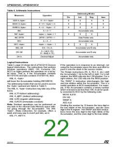
Registers
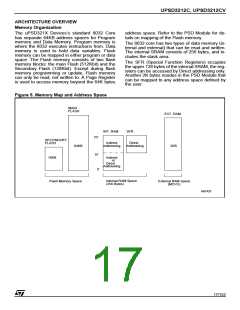
The 8032 has several registers; these are the Pro-
gram Counter (PC), Accumulator (A), B Register
(B), the Stack Pointer (SP), the Program Status
Word (PSW), General purpose registers (R0 to
R7), and DPTR (Data Pointer register).
Accumulator. The Accumulator is the 8-bit gen-
eral purpose register, used for data operation such
as transfer, temporary saving, and conditional
tests. The Accumulator can be used as a 16-bit
register with B Register as shown in Figure 6.
the BIT instruction is executed, Bit 6 of memory is
copied to this flag.
[Parity Flag, P]. This flag reflects on number of Ac-
cumulator’s “1.” If the number of Accumulator’s 1
is odd, P=0. otherwise, P=1. The sum of adding
Accumulator’s 1 to P is always even.
R0~R7. General purpose 8-bit registers that are
locked in the lower portion of internal data area.
Data Pointer Register. Data Pointer Register is
16-bit wide which consists of two-8bit registers,
DPH and DPL. This register is used as a data
pointer for the data transmission with external data
memory in the PSD Module.
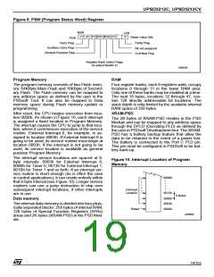
B Register. The B Register is the 8-bit general
purpose register, used for an arithmetic operation
such as multiply, division with the Accumulator
(see Figure 7).
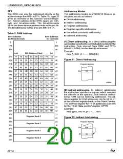
Stack Pointer. The Stack Pointer Register is 8
bits wide. It is incremented before data is stored
during PUSH and CALL executions. While the
stack may reside anywhere in on-chip RAM, the
Stack Pointer is initialized to 07h after reset. This
causes the stack to begin at location 08h (see Fig-
ure 8).
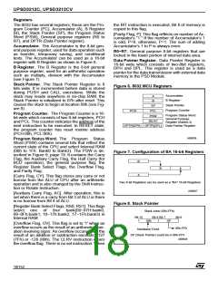
Figure 6. 8032 MCU Registers
Accumulator
B Register
A
B
Stack Pointer
SP
PCL
Program Counter
PCH
Program Counter. The Program Counter is a 16-
bit wide which consists of two 8-bit registers, PCH
and PCL. This counter indicates the address of the
next instruction to be executed. In RESET state,
the program counter has reset routine address
(PCH:00h, PCL:00h).
Program Status Word
General Purpose
Register (Bank0-3)
PSW
R0-R7
DPTR(DPH) DPTR(DPL) Data Pointer Register
AI06636
Program Status Word. The Program Status
Word (PSW) contains several bits that reflect the
current state of the CPU and select Internal RAM
(00h to 1Fh: Bank0 to Bank3). The PSW is de-
scribed in Figure 9, page 19. It contains the Carry
Flag, the Auxiliary Carry Flag, the Half Carry (for
BCD operation), the general purpose flag, the
Register Bank Select Flags, the Overflow Flag,
and Parity Flag.
[Carry Flag, CY]. This flag stores any carry or not
borrow from the ALU of CPU after an arithmetic
operation and is also changed by the Shift Instruc-
tion or Rotate Instruction.
Figure 7. Configuration of BA 16-bit Registers
B
B
A
A
Two 8-bit Registers can be used as a "BA" 16-bit Registers
AI06637
[Auxiliary Carry Flag, AC]. After operation, this is
set when there is a carry from Bit 3 of ALU or there
is no borrow from Bit 4 of ALU.
Figure 8. Stack Pointer
[Register Bank Select Flags, RS0, RS1]. This flags
select one of
four bank(00~07H:bank0,
Stack Area (30h-FFh)
08~0Fh:bank1, 10~17h:bank2, 17~1Fh:bank3) in
Internal RAM.
Bit 15
Bit 8 Bit 7
Bit 0
00h
SP
[Overflow Flag, OV]. This flag is set to '1' when an
overflow occurs as the result of an arithmetic oper-
ation involving signs. An overflow occurs when the
result of an addition or subtraction exceeds +127
(7Fh) or -128 (80h). The CLRV instruction clears
the overflow flag. There is no set instruction. When
00h-FFh
Hardware Fixed
SP (Stack Pointer) could be in 00h-FFh
AI06638
18/152

 STMICROELECTRONICS [ ST ]