UPSD3212C, UPSD3212CV
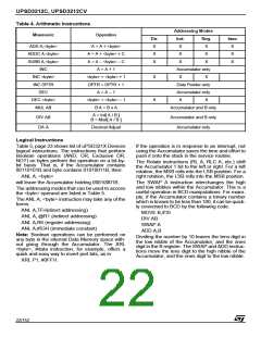
Table 4. Arithmetic Instructions
Mnemonic
Addressing Modes
Operation
Dir.
X
Ind.
X
Reg.
X
Imm
X
ADD A,<byte>
A = A + <byte>
ADDC A,<byte>
SUBB A,<byte>
INC
A = A + <byte> + C
A = A – <byte> – C
A = A + 1
X
X
X
X
X
X
X
X
Accumulator only
INC <byte>
INC DPTR
DEC
<byte> = <byte> + 1
DPTR = DPTR + 1
A = A – 1
X
X
X
X
Data Pointer only
Accumulator only
DEC <byte>
MUL AB
<byte> = <byte> – 1
B:A = B x A
X
X
Accumulator and B only
Accumulator and B only
Accumulator only
A = Int[ A / B ]
B = Mod[ A / B ]
DIV AB
DA A
Decimal Adjust
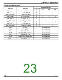
Logical Instructions
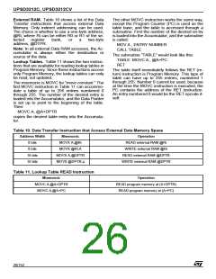
Table 5, page 23 shows list of uPSD321X Devices
logical instructions. The instructions that perform
Boolean operations (AND, OR, Exclusive OR,
NOT) on bytes perform the operation on a bit-by-
bit basis. That is, if the Accumulator contains
00110101B and byte contains 01010011B, then:
If the operation is in response to an interrupt, not
using the Accumulator saves the time and effort to
push it onto the stack in the service routine.
The Rotate instructions (RL A, RLC A, etc.) shift
the Accumulator 1 bit to the left or right. For a left
rotation, the MSB rolls into the LSB position. For a
right rotation, the LSB rolls into the MSB position.
ANL A, <byte>
will leave the Accumulator holding 00010001B.
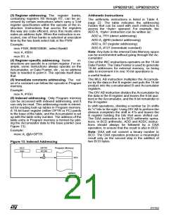
The addressing modes that can be used to access
the <byte> operand are listed in Table 5.
The ANL A, <byte> instruction may take any of the
forms:
The SWAP A instruction interchanges the high
and low nibbles within the Accumulator. This is a
useful operation in BCD manipulations. For exam-
ple, if the Accumulator contains a binary number
which is known to be less than 100, it can be quick-
ly converted to BCD by the following code:
ANL A,7FH(direct addressing)
ANL A, @R1 (indirect addressing)
ANL A,R6 (register addressing)
ANL A,#53H (immediate constant)
MOVE B,#10
DIV AB
SWAP A
ADD A,B
Note: Boolean operations can be performed on
any byte in the internal Data Memory space with-
out going through the Accumulator. The XRL
<byte>, #data instruction, for example, offers a
quick and easy way to invert port bits, as in
Dividing the number by 10 leaves the tens digit in
the low nibble of the Accumulator, and the ones
digit in the B register. The SWAP and ADD instruc-
tions move the tens digit to the high nibble of the
Accumulator, and the ones digit to the low nibble.
XRL P1, #0FFH.
22/152

 STMICROELECTRONICS [ ST ]