UPSD3212C, UPSD3212CV
MAXIMUM RATING
Stressing the device above the rating listed in the
Absolute Maximum Ratings” table may cause per-
manent damage to the device. These are stress
ratings only and operation of the device at these or
any other conditions above those indicated in the
Operating sections of this specification is not im-
plied. Exposure to Absolute Maximum Rating con-
ditions for extended periods may affect device
reliability. Refer also to the STMicroelectronics
SURE Program and other relevant quality docu-
ments.
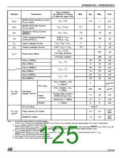
Table 85. Absolute Maximum Ratings
Symbol
Parameter
Min.
Max.
125
235
6.5
Unit
°C
°C
V
T
Storage Temperature
–65
STG
(1)
TLEAD
VIO
Lead Temperature during Soldering (20 seconds max.)
Input and Output Voltage (Q = V or Hi-Z)
–0.5
–0.5
OH
V
CC
Supply Voltage
6.5
V
V
Device Programmer Supply Voltage
–0.5
14.0
2000
V
PP
2
VESD
–2000
V
Electrostatic Discharge Voltage (Human Body Model)
Note: 1. IPC/JEDEC J-STD-020A
2. JEDEC Std JESD22-A114A (C1=100pF, R1=1500 Ω, R2=500 Ω)
121/152

 STMICROELECTRONICS [ ST ]