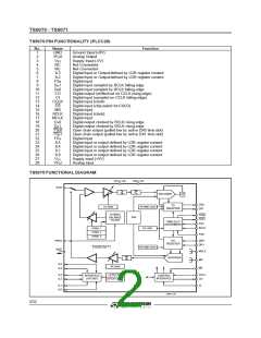
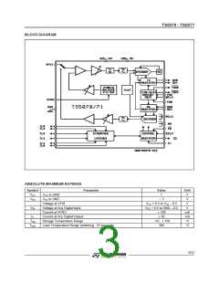
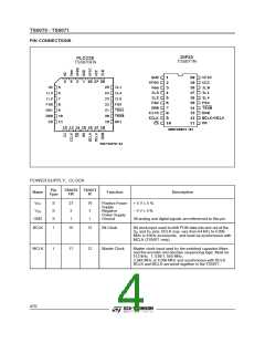
TS5070 - TS5071
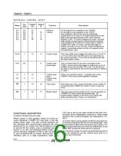
INTERFACE, CONTROL, RESET
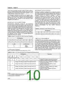
Pin
Type
TS5070 TS5071
Name
Function
Description
FN
N
IL5
IL4
IL3
IL2
IL1
IL0
I/O
I/O
I/O
I/O
I/O
I/O
23
24
6
7
25
–
16
4
5
17
Interface
Latches
IL5 through IL0 are available on the TS5070,
IL4 through IL0 are available on the TS5071.
Each interface Latch I/O pin may be individually
programmed as an input or an output determined by the
state of the corresponding bit in the Latch Direction
Register (LDR) . For pins configured as inputs, the logic
state sensed on each input is latched into the interface
Latch Register (ILR) whenever control data is written to
COMBO IIG, while CS is low, and the information is
shifted out on the CO (or CI/O) pin. When configured as
outputs, control data written into the ILR appears at the
corresponding IL pins.
26
18
CCLK
CI/O
I
13
–
9
8
Control Clock
This clock shifts serial control information into or out of CI
or CO (or CI/O) when the CS input is low depending on
the current instruction. CCLK may be asynchronous with
the other system clocks.
I/O
Control Data
Input/output
This is Control Data I/O pin wich is provided on the
TS5071. Serial control information is shifted into or out of
COMBO IIG on this pin when CS is low. The direction of
the data is determined by the current instruction as defined
in Table 1.
CI
I
12
11
–
–
Control Data
Input
Control Data
These are separate controls, availables only on the
TS5070. They can be wired together if required.
CO
O
Output
CS
I
I
14
15
10
11
Chip Select
When this pins is low, control information can be written to
or read from the COMBO IIG via the CI and CO pins (or
CI/O).
MR
Master Reset
This logic input must be pulled low for normal operation of
COMBO IIG. When pulled momentarily high, all
programmable registers in the device are reset to the
states specified under ”Power–on Initialization”.
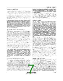
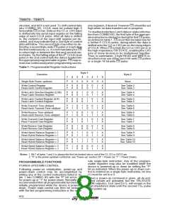
CI/O pin is set as an input ready for the first con-
trol byte of the initialization sequence. Other initial
states in the Control Register are indicated in Ta-
ble 2.
A resetto thesesameinitial conditionsmayalso be
forcedby drivingtheMR pinmomentarilyhigh. This
may be doneeitherwhen powered-upor down.For
normal operationthis pin must be pulled low. If not
used, MR should be hard-wired to ground.
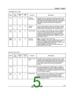
FUNCTIONAL DESCRIPTION
POWER-ON INITIALIZATION
When power is first applied, power-on reset cir-
cuitry initializes COMBO IIG and puts it into the
power-down state. The gain control registers for
the transmit and receive gain sections are pro-
grammed for no output, the hybrid balance circuit
is turned off, the power amp is disabled and the
device is in the non-delayed timing mode. The
Latch Direction Register (LDR) is pre-set with all
IL pins programmed as inputs, placing the SLIC
interface pins in a high impedance state. The
The desired modes for all programmablefunctions
may be initialized via the control port prior to a
Power-up command.
6/32

 STMICROELECTRONICS [ ST ]