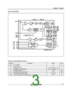
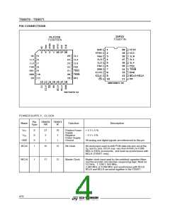
TS5070 - TS5071
Register,isincluded,andfinallya Post-Filter/Power
POWER-DOWN STATE
Ω
±
Amplifier capable of driving a 300 load to 3.5
V, a 600 Ω load to ± 3.8 V or 15 kΩ load to ± 4.0 V
at peak overload.
Following a period of activity in the powered-up
state the power-down state may be re-entered by
writing any of the control instructions into the serial
control port with the ”P” bit set to ”1” It is recom-
mendedthat the chipbe powered downbefore writ-
ing any additional instructions. In the power-down
state, all non-essential circuitry is de-activated and
the DX0 andDX1 outputsare in the high impedance
TRI-STATE condition.
A decode cycle begins immediately after each re-
µ
ceive time-slot, and 10 s later the Decoder DAC
µ
output is updated. The total signal delay is 10 s
plus 120 µs (filter delay) plus 62.5 µs (1/2 frame)
which gives approximately 190 µs.
The coefficientsstoredin theHybridBalancecircuit
and the Gain Control registers,the data in the LDR
and ILR, and all control bits remain unchanged in
the power-down state unless changed by writing
new data via the serial control port, which remains
operational. The outputs of the Interface Latches
also remain active, maintaining the ability to moni-
tor and control a SLIC.
PCM INTERFACE
The FSX and FSR frame sync inputsdetermine the
beginning of the 8-bit transmit and receive time-
slots respectively. They may have any duration
from a single cycle of BCLK to one MCLK period
LOW. Two different relationships may be estab-
lishedbetweentheframesyncinputsand theactual
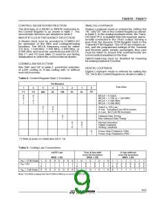
time-slotson thePCM bussesby settingbit 3 inthe
Control Register (see table 2). Non delayed data
mode is similar to long-frame timing on the
ETC5050/60 series of devices : time-slots being
nominallycoincident with the rising edge of the ap-
propriate FS input. The alternative is to use De-
layed Data mode which is similar to short-frame
sync timing, in which each FS input must be high
at least a half-cycle of BCLK earlier than the time-
slot.
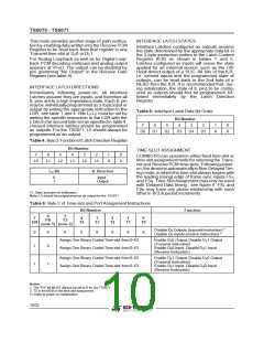
TheTime-SlotAssignmentcircuit on thedevicecan
onlybe usedwithDelayedData timing.Whenusing
Time-Slot Assignment, the beginning of the first
time-slot in a frame is identifiedby the appropriate
FSinput.Theactualtransmitandreceivetime-slots
are then determined by the internal Time-Slot As-
signment counters. Transmit and Receive frames
and time-slots may be skewed from each other by
any number of BCLK cycles.
TRANSMIT FILTER AND ENCODER
The Transmit section input, VFXI, is a high imped-
ance summinginputwhichis usedas thedifferenc-
ing pointfortheinternalhybridbalancecancellation
signal. No external componentsare needed to set
the gain. Following this circuit is a programmable
gain/attenuationamplifier whichis controlledbythe
contents of the Transmit Gain Register (see Pro-
grammable Functions section). An active prefilter
then precedes the 3rd order high-pass and 5th or-
der low-pass switched capacitor filters. The A/D
converterhas acompressingcharacteristicaccord-
µ
ing to the standard CCITT A or 255 coding laws,
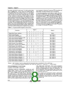
which mustbe selectedbya controlinstructiondur-
ing initialization(see table 1 and 2). A precisionon-
chip voltagereferenceensuresaccurateand highly
stable transmission levels. Any offset voltage aris-
ing in the gain-set amplifier, the filters or the com-
paratoris cancelledbyan internalauto-zerocircuit.
During each assigned transmit time-slot, the se-
lected DX0/1 output shifts data out from the PCM
register on the rising edges of BCLK. TSX0 (or
TSX1 as appropriate) also pulls low for the first 7
1/2 bit times of the time-slot to control the TRI-
STATE Enable of a backplane line driver. Serial
PCM data is shifted into the selected DR0/1 input
during each assigned Receive time slot on the
falling edges of BCLK. DX0 or DX1 and DR0 or
DR1 are selectable on the TS5070 only.
Each encode cycle begins immediately following
the assigned Transmit time-slot. The total signal
delay referenced to the start of the time-slot is ap-
µ
proximately 165 s (due to the Transmit Filter)
plus 125 µs (due to encoding delay), which totals
290 µs. Data is shifted out on DX0 or DX1 during
the selected time slot on eight rising edges of
BCLK.
SERIAL CONTROL PORT
DECODER AND RECEIVE FILTER
Control information and data are written into or
readback from COMBO IIG via the serial control
portconsistingof the controlclockCCLK; theserial
data input/output CI/O (or separate input CI, and
output CO on the TS5070only) ; and the Chip Se-
lect input CS. All control instructions require 2
bytes,as listedintable1, withtheexceptionof asin-
gle bytepower-up/downcommand. The byte 1 bits
are used as follows: bit 7 specifies power-up or
power-down; bits 6, 5, 4 and 3 specify the register
address; bit 2 specifies whether the instructions is
read or write; bit 1 specifies a one or two byte in-
PCM data is shifted into the Decoder’s Receive
PCM Registervia the DR0 or DR1 pin duringthe se-
lected time-sloton the 8 fallingedgesof BCLK.The
Decoder consists of an expandingDAC with either
µ
A or 255 law decodingcharacteristic, which is se-
lectedby thesamecontrolinstructionusedtoselect
the Encode law during initialization. Following the
Decoder is a 5thorderlow-pass switched capacitor
filter with integral Sin x/x correction for the 8 kHz
sample and hold. A programmable gain amplifier,
which must be set by writing to the Receive Gain
7/32

 STMICROELECTRONICS [ ST ]