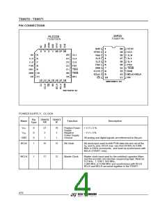
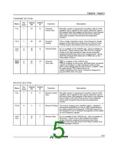
TS5070 - TS5071
TRANSMIT SECTION
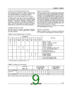
Pin
Type
TS5070 TS5071
Name
Function
Transmit
Description
FN
N
FSX
I
22
15
Normally a pulse or squarewave waveform with an 8 kHz
repetition rate is applied to this input to definethe start of
the transmit time-slot assigned to this device (non-delayed
data mode) or the start of the transmit frame (delayed
data mode using the internal time-slot assignment
counter).
Frame Sync.
VFXI
I
28
20
Transmit
Analog
This is a high–impedance input. Voice frequency signals
present on this input are encoded as an A–law or µ–law
PCM bit stream and shifted out on the selected DX pin.
DX0
DX1
0
0
18
19
13
–
Transmit Data
DX1 is available on theTS5070 only, DX0 is available on
all devices. These transmit data TRI–STATE outputs
remain in the high impedance state except during the
assigned transmit time–slot on the assigned port, during
which the transmit PCM data byte is shifted out on the
rising edges of BCLK.
TSX0
TSX1
0
0
20
21
14
–
Transmit
Time–slot
TSX1 is available on the TS5070 only.
TSX0 is available on all devices. Normally these opendrain
outputs are floating in a high impedance state except
when a time–slot is active on one of the DX outputs, when
the apppropriate TSX output pulls low to
enable a backplane line–driver. Should be strapped to
ground (GND) when not used.
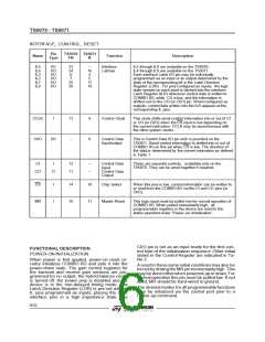
RECEIVE SECTION
Pin
Type
TS5070 TS5071
Name
Function
Description
FN
N
FSR
I
8
6
Receive Frame Normally a pulse or squarewave waveform with an 8 kHz
Sync.
repetition rate is applied to this input to definethe start of
the receive time–slot assigned to this device (non-delayed
frame mode) or the start of the receive frame (delayed
frame mode using the internal time-slot assignment
counter.
VFR0
0
2
2
Receive Analog The receive analog power amplifier output, capable of
driving load impedances as low as 300 (depending on
Ω
the peak overload levelrequired). PCM data received on
the assigned DR pin is decoded and appears at this output
as voice frequency signals.
DR0
DR1
I
I
10
9
7
–
Receive Data
DR1 is available on the TS5070 only, DR0 is available on
all devices. These receive data input(s) are inactive
except during the assigned receive time–slot of the
assigned port when the receive PCM data is shifted in on
the falling edges of BCLK.
5/32

 STMICROELECTRONICS [ ST ]