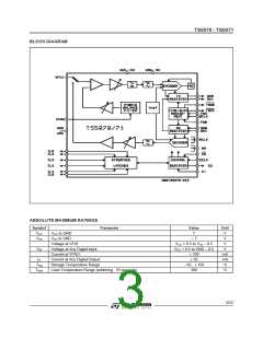
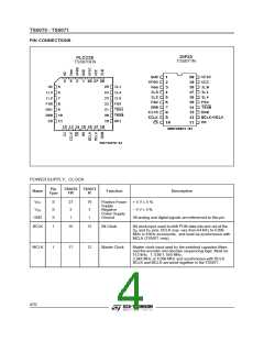
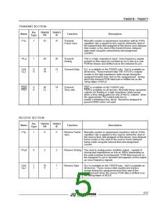
TS5070 - TS5071
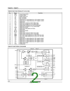
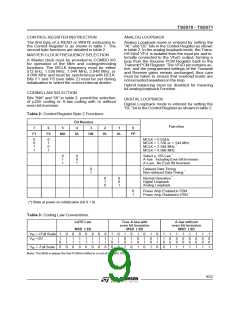
PIN CONNECTIONS
DIP20
TS5071N
PLCC28
TS5070FN
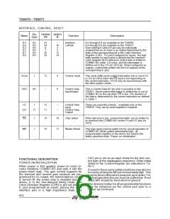
POWER SUPPLY, CLOCK
Pin
Type
TS5070 TS5071
Name
Function
Description
FN
N
VCC
VSS
S
S
S
27
3
19
3
Positive Power
Supply
Negative
Power Supply
Ground
+ 5 V ± 5 %
– 5 V ± 5 %
GND
1
1
All analog and digital signals are referenced to this pin.
BCLK
MCLK
I
16
17
12
12
Bit Clock
Bit clock input used to shift PCM data into and out of the
DR and DX pins. BCLK may vary from 64 kHz to 4.096
MHz in 8 kHz increments, and must be synchronous with
MCLK (TS5071 only).
I
Master Clock
Master clock input used by the switched capacitor filters
and the encoder and decoder sequencing logic. Must be
512 kHz, 1. 536/1. 544 MHz,
2.048 MHz or 4.096 MHz and synchronous with BCLK.
BCLK and MCLK are wired together in the TS5071.
4/32

 STMICROELECTRONICS [ ST ]