TS5070 - TS5071
This mode provides another stage of path verifica-
tionby enablingdata written into the ReceivePCM
Register to be read back from that register in any
Transmit time-slot at DX0 or DX1.
For Analog Loopback as well as for Digital Loop-
back PCM decoding continues and analog output
appears at VFRO. The output can be disabled by
pro gramming ”No Output” in the Receive Gain
Register (see table 8).
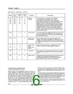
INTERFACE LATCH STATES
Interface Latches configured as outputs assume
the state determined by the appropriate data bit in
the 2-byte instruction written to the Latch Content
Register (ILR) as shown in tables 1 and 5.
Latches configured as inputs will sense the state
applied by an external source, such as the Off-
Hook detect output of a SLIC. All bits of the ILR,
i.e. sensed inputs and the programmed state of
outputs, can be read back in the 2nd byte of a
READ from the ILR. It is recommended that, dur-
ing initialization, the state of IL pins to be config-
ured as outputs should first be programmed, fol-
lowed immediately by the Latch Direction
Register.
INTERFACE LATCH DIRECTIONS
Immediately following power-on, all Interface
Latches assume they are inputs, and therefore all
IL pins are in a high impedance state. Each IL pin
maybe individuallyprogrammed as a logicinput or
output by writing the appropriateinstruction to the
LDR, see table 1 and 4. Bits L5-L0 must be set by
writing the specific instruction to the LDR with the
L bits in the secondbyte set as specifiedin table4.
Unused interface latches should be programmed
as outputs.For the TS5071, L5 should always be
programmed as an output.
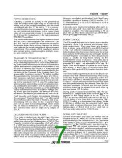
Table 5: Interface Latch Data Bit Order
Bit Number
7
6
5
4
3
2
1
0
D0
D1
D2
D3
D4
D5
X
X
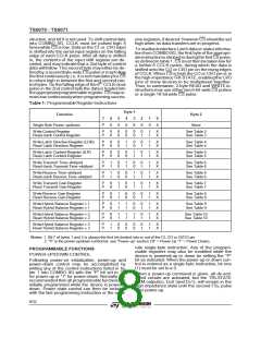
Table 4: Byte2 Functionof LatchDirection Register
Bit Number
TIME-SLOT ASSIGNMENT
7
6
5
4
3
2
1
0
COMBO IIGcan operatein either fixed time-slot or
time-slot assignmentmode for selectingthe Trans-
mit and ReceivePCM time-slots. Followingpower-
on,the deviceis automaticallyin Non-DelayedTim-
ing mode,in whichthe time-slotalwaysbegins with
the leading (rising) edge of frame sync inputs FSX
and FSR. Time-Slot Assignment may only be used
with Delayed Data timing : see figure 6. FSX and
FSR may have any phase relationship with each
other in BCLK period increments.
L0
L1
L2
L3
L4
L5
X
X
LN Bit
IL Direction
0
1
Input *
Output
(*) State at power-on initilization.
Note: L5 should be programmed as an output for the TS5071.
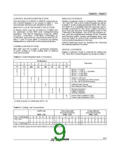
Table 6: Byte 2 of Time-slot and Port Assignment Instructions
Bit Number
Function
6
PS
5
T5
7
EN
4
T4
3
T3
2
T2
1
T1
0
T0
(note 1) (note 2)
Disable DX Outputs (transmit instruction) *
Disable DR Inputs (receive instruction) *
0
1
X
0
X
X
X
X
X
X
Assign One Binary Coded Time-slot from 0–63
Assign One Binary Coded Time-slot from 0–63
Enable DX0 Output, Disable DX1 Output
(Transmit instruction)
Enable DR0 Input, Disable DR1 Input
(Receive Instruction)
Assign One Binary Coded Time-slot from 0–63
Assign One Binary Coded Time-slot from 0–63
Enable DX1 Output, Disable DX0 Output
(Transmit instruction)
Enable DR1 Input, Disable DR0 Input
(Receive Instruction)
1
1
Notes:
1. The ”PS” bit MUST always be set to 0 for the TS5071.
2. T5 is the MSB of the time-slot assignment.
(*) State at power-on initialization
10/32

 STMICROELECTRONICS [ ST ]