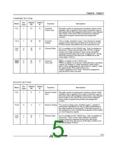
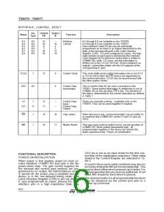
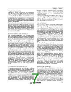
TS5070 - TS5071
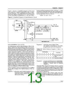
CONTROL REGISTER INSTRUCTION
ANALOG LOOPBACK
The first byte of a READ or WRITE instruction to
the Control Register is as shown in table 1. The
second byte functions are detailed in table 2.
Analog Loopback mode is entered by setting the
”AL” and ”DL” bits in the Control Registeras shown
in table 2. In the analog loopbackmode, the Trans-
mit input VFXI is isolated from the input pin and in-
ternally connected to the VFRO output, forming a
loop from the Receive PCM Register back to the
Transmit PCM Register. The VFRO pin remains ac-
tive, and the programmed settings of the Transmit
and Receive gains remain unchanged, thus care
must be taken to ensure that overload levels are
notexceededanywherein the loop.
MASTER CLOCK FREQUENCY SELECTION
A Master clock must be provided to COMBO IIG
for operation of the filter and coding/decoding
functions. The MCLK frequency must be either
512 kHz, 1.536 MHz, 1.544 MHz, 2.048 MHz, or
4.096 MHz and must be synchronous with BCLK.
Bits F1 and F0 (see table 2) must be set during
initialization to select the correct internal divider.
Hybrid balancing must be disabled for meaning
ful analog loopback Function.
CODING LAW SELECTION
Bits ”MA” and ”IA” in table 2 permit the selection
of µ255 coding or A-law coding with or without
even-bit inversion.
DIGITAL LOOPBACK
Digital Loopback mode is entered by setting the
”DL”bit in the ControlRegister as shown in table 2.
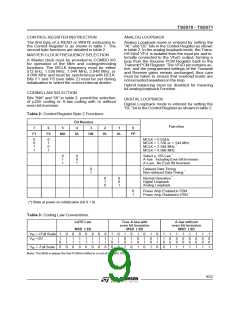
Table 2: ControlRegister Byte 2 Functions
Bit Number
Function
0
7
6
5
4
3
2
1
F1
F0
MA
IA
DN
DL
AL
PP
0
0
1
1
0
1
0
1
MCLK = 512 kHz
MCLK = 1. 536 or 1. 544 MHz
MCLK = 2. 048 MHz *
MCLK = 4. 096 MHz
0
1
1
X
0
1
Select µ. 255 Law *
A–law, Including Even Bit Inversion
A–Law, No Even Bit Inversion
0
1
Delayed Data Timing
Non–delayed Data Timing *
0
1
0
0
X
1
Normal Operation *
Digital Loopback
Analog Loopback
0
1
Power Amp Enabled in PDN
Power Amp Disabled in PDN *
(*) State at power-on initialization (bit 4 = 0)
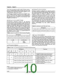
Table 3: Coding Law Conventions.
m255 Law
True A-law with
even bit inversion
MSB LSB
A-law without
even bit inversion
MSB LSB
MSB LSB
V
IN = +Full Scale
1
0
0
0
0
0
0
0
1
0
1
0
1
0
1
0
1
1
1
1
1
1
1
1
VIN = 0V
1
0
1
1
1
1
1
1
1
1
1
1
1
1
1
1
1
0
1
1
0
0
1
1
0
0
1
1
0
0
1
1
1
0
0
0
0
0
0
0
0
0
0
0
0
0
0
0
VIN = -Full Scale
0
0
0
0
0
0
0
0
0
0
1
0
1
0
1
0
0
1
1
1
1
1
1
1
Note: The MSB is always the first PCM bit shifted in or out of COMBO IIG.
9/32

 STMICROELECTRONICS [ ST ]