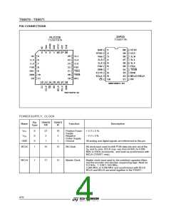
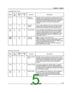
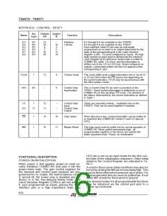
TS5070 - TS5071
struction;and bit 0 is not used. To shiftcontroldata
into COMBO IIG, CCLK must be pulsed high 8
timeswhile CS is low. Data on the CI or CI/Oinput
is shifted into the serial input register on the falling
edge of each CCLK pulse. After all data is shifted
in, the contents of the input shift register are de-
coded, and may indicate that a 2nd byte of control
data will follow. Thissecondbyte mayeither be de-
finedby asecondbyte-wideCS pulseor mayfollow
the first continuously,i.e. it is not mandatoryfor CS
to return high in between the first and second con-
trol bytes.On thefalling edgeof the8th CCLKclock
pulse in the 2nd control byte the datais loadedinto
theappropriateprogrammableregister.CS mayre-
main low continuouslywhen programmingsucces-
siveregisters,if desired.HoweverCS shouldbe set
high when no data transfers are in progress.
To readbackinterfaceLatch dataor statusinforma-
tion from COMBOIIG, the first byte of the appropri-
ateinstructionisstrobedinduringthe firstCSpulse,
as definedin table1. CS must thenbe takenlow for
a further 8 CCLK cycles, during which the data is
shifted onto the CO or CI/O pin on the rising edges
of CCLK. When CS is high the CO or CI/O pin is in
the high-impedanceTRI-STATE, enablingthe CI/O
pins of many devices to be multiplexed together.
Thus, to summarize, 2-byte READ and WRITE in-
structionsmay use either two 8-bit wide CS pulses
or a single 16-bit wide CS pulse.
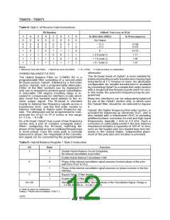
Table 1: ProgrammableRegister Instructions
Byte 1
Function
Byte 2
7
6
5
4
3
2
1
0
Single Byte Power–up/down
P
X
X
X
X
X
0
X
None
Write Control Register
Read–back Control Register
P
P
0
0
0
0
0
0
0
0
0
1
1
1
X
X
See Table 2
See Table 2
Write Latch Direction Register (LDR)
Read Latch Direction Register
P
P
0
0
0
0
1
1
0
0
0
1
1
1
X
X
See Table 4
See Table 4
Write Latch Content Register (ILR)
Read Latch Content Register
P
P
0
0
0
0
0
0
1
1
0
1
1
1
X
X
See Table 5
See Table 5
Write Transmit Time–slot/port
Read–back Transmit Time–slot/port
P
P
1
1
0
0
1
1
0
0
0
1
1
1
X
X
See Table 6
See Table 6
Write Receive Time–slot/port
Read–back Receive Time–slot/port
P
P
1
1
0
0
0
0
1
1
0
1
1
1
X
X
See Table 6
See Table 6
Write Transmit Gain Register
Read Transmit Gain Register
P
P
0
0
1
1
0
0
1
1
0
1
1
1
X
X
See Table 7
See Table 7
Write Receive Gain Register
Read Receive Gain Register
P
P
0
0
1
1
0
0
0
0
0
1
1
1
X
X
See Table 8
See Table 8
Write Hybrid Balance Register ≠ 1
Read Hybrid Balance Register ≠ 1
P
P
0
0
1
1
1
1
0
0
0
1
1
1
X
X
See Table 9
See Table 9
Write Hybrid Balance Register
Read Hybrid Balance Register ≠ 2
2
P
P
0
0
1
1
1
1
1
1
0
1
1
1
X
X
See Table 10
See Table 10
≠
Write Hybrid Balance Register ≠ 3
P
P
1
1
0
0
0
0
0
0
0
1
1
1
X
X
Read Hybrid Balance Register
3
≠
Notes: 1. Bit 7 of bytes 1 and 2 is always the first bit clocked into or out of the CI, CO or CI/CO pin.
2. ”P” is the power-up/down control bit, see ”Power-up” section (”0” = Power Up ”1” = Power Down).
rate single-byte instruction. Any of the program-
PROGRAMMABLE FUNCTIONS
POWER-UP/DOWN CONTROL
mable registers may also be modified while the
device is powered-up or down be setting the ”P”
bit as indicated. When the power up or down con-
trol is entered as a single byte instruction, bit one
(1) must be set to a 0.
When a power-up command is given, all de-acti-
vated circuits are activated, but the TRI-STATE
PCM output(s), DX0 (and DX1), will remain in the
high impedance state until the second FSX pulse
after power-up.
Following power-on initialization, power-up and
power-down control may be accomplished by
writing any of the control instructions listed in ta-
ble 1 into COMBO IIG with the ”P” bit set to ”0”
for power-up or ”1” for power-down. Normally it is
recommended that all programmable functions be
initially programmed while the device is powered
down. Power state control can then be included
with the last programming instruction or the sepa-
8/32

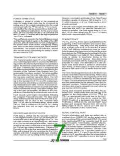
 STMICROELECTRONICS [ ST ]