STM32F105xx, STM32F107xx
Electrical characteristics
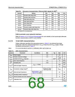
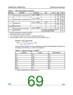
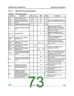
Table 51. ADC characteristics (continued)
Symbol
Parameter
Conditions
Min
Typ
Max
Unit
fADC = 14 MHz
0.214
3(4)
µs
1/fADC
µs
(2)
tlat
Injection trigger conversion latency
fADC = 14 MHz
fADC = 14 MHz
0.143
2(4)
(2)
tlatr
Regular trigger conversion latency
1/fADC
µs
0.107
1.5
0
17.1
239.5
1
(2)
tS
Sampling time
Power-up time
1/fADC
µs
(2)
tSTAB
0
fADC = 14 MHz
1
18
µs
Total conversion time (including
sampling time)
(2)
tCONV
14 to 252 (tS for sampling +12.5 for
successive approximation)
1/fADC
1. Based on characterization, not tested in production.
2. Guaranteed by design, not tested in production.
3. VREF+ is internally connected to VDDA and VREF- is internally connected to VSSA
.
4. For external triggers, a delay of 1/fPCLK2 must be added to the latency specified in Table 51.
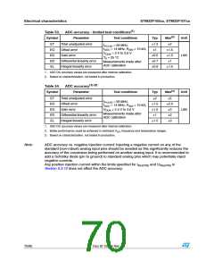
Equation 1: R
max formula
TS
AIN
RAIN > -------------------------------------------------------------- – RADC
fADC · CADC · ln*2N + 2
+
The formula above (Equation 1) is used to determine the maximum external impedance allowed for an
error below 1/4 of LSB. Here N = 12 (from 12-bit resolution).
(1)
Table 52.
R
max for f
= 14 MHz
AIN
ADC
Ts (cycles)
tS (µs)
RAIN max (kY)
1.5
0.11
0.4
7.5
0.54
0.96
2.04
2.96
3.96
5.11
17.1
5.9
13.5
28.5
41.5
55.5
71.5
239.5
11.4
25.2
37.2
50
NA
NA
1. Based on characterization, not tested in production.
Doc ID 15274 Rev 4
69/95

 STMICROELECTRONICS [ ST ]