STM32F105xx, STM32F107xx
Electrical characteristics
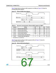
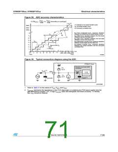
Figure 29. ADC accuracy characteristics
VREF+
VDDA
4096
[1LSBIDEAL
=
(or
depending on package)]
4096
EG
(1) Example of an actual transfer curve
4095
4094
4093
(2) The ideal transfer curve
(3) End point correlation line
(2)
ET=Total Unadjusted Error: maximum deviation
between the actual and the ideal transfer curves.
ET
(3)
7
6
5
4
3
2
1
EO=Offset Error: deviation between the first actual
transition and the first ideal one.
(1)
EG=Gain Error: deviation between the last ideal
transition and the last actual one.
EO
EL
ED=Differential Linearity Error: maximum deviation
between actual steps and the ideal one.
EL=Integral Linearity Error: maximum deviation
between any actual transition and the end point
correlation line.
ED
1 LSBIDEAL
0
1
2
3
4
5
6
7
4093 4094 4095 4096
VDDA
VSSA
ai14395b
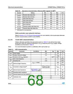
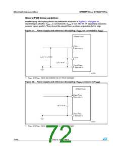
Figure 30. Typical connection diagram using the ADC
STM32F10xxx
V
DD
Sample and hold ADC
converter
V
T
0.6 V
(1)
C
(1)
R
R
AIN
ADC
AINx
12-bit
converter
V
T
0.6 V
V
AIN
C
(1)
ADC
parasitic
I
1 µA
L
ai14139d
1. Refer to Table 51 for the values of RAIN, RADC and CADC
.
2. Cparasitic represents the capacitance of the PCB (dependent on soldering and PCB layout quality) plus the
pad capacitance (roughly 7 pF). A high Cparasitic value will downgrade conversion accuracy. To remedy
this, fADC should be reduced.
Doc ID 15274 Rev 4
71/95

 STMICROELECTRONICS [ ST ]