STM32F105xx, STM32F107xx
Electrical characteristics
USB OTG FS characteristics
The USB OTG interface is USB-IF certified (Full-Speed).
Table 44. USB OTG FS startup time
Symbol
Parameter
Max
Unit
(1)
tSTARTUP
USB OTG FS transceiver startup time
1
µs
1. Guaranteed by design, not tested in production.
Table 45. USB OTG FS DC electrical characteristics
Symbol
Parameter
Conditions
Min.(1) Typ. Max.(1) Unit
USB OTG FS operating
voltage
VDD
3.0(2)
0.2
3.6
V
(3)
VDI
Differential input sensitivity
I(USBDP, USBDM)
Includes VDI range
Input
levels
Differential common mode
range
(3)
VCM
0.8
2.5
2.0
V
Single ended receiver
threshold
(3)
VSE
1.3
VOL Static output level low
VOH Static output level high
RL of 1.5 kY to 3.6 V(4)
0.3
3.6
Output
levels
V
(4)
RL of 15 kY to VSS
2.8
17
Pull-down resistance on
PA11, PA12
21
24
RPD
VIN = VDD
Pull-down resistance on
PA9
0.65
1.5
1.1
1.8
2.0
2.1
kY
Pull-up resistance on PA12
Pull-up resistance on PA9
VIN = VSS
VIN = VSS
RPU
0.25 0.37 0.55
1. All the voltages are measured from the local ground potential.
2. The STM32F105xx and STM32F107xx USB OTG FS functionality is ensured down to 2.7 V but not the full
USB OTG FS electrical characteristics which are degraded in the 2.7-to-3.0 V VDD voltage range.
3. Guaranteed by design, not tested in production.
RL is the load connected on the USB OTG FS drivers
4.
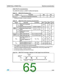
Figure 25. USB OTG FS timings: definition of data signal rise and fall time
Crossover
points
Differential
data lines
V
CR S
V
SS
t
t
r
f
ai14137
Doc ID 15274 Rev 4
65/95

 STMICROELECTRONICS [ ST ]