Electrical characteristics
STM32F105xx, STM32F107xx
(1)
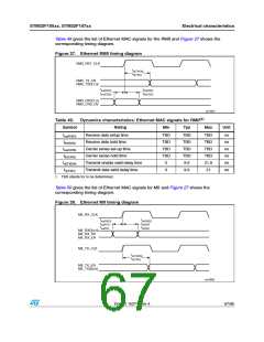
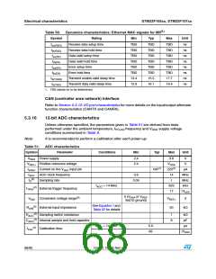
Table 50. Dynamics characteristics: Ethernet MAC signals for MII
Symbol
Rating
Min
Typ
Max
Unit
tsu(RXD)
tih(RXD)
tsu(DV)
tih(DV)
Receive data setup time
Receive data hold time
Data valid setup time
Data valid hold time
TBD
TBD
TBD
TBD
TBD
TBD
13.4
12.9
TBD
TBD
TBD
TBD
TBD
TBD
15.5
16.1
TBD
TBD
TBD
TBD
TBD
TBD
17.7
19.4
ns
ns
ns
ns
ns
ns
ns
ns
tsu(ER)
tih(ER)
td(TXEN)
td(TXD)
Error setup time
Error hold time
Transmit enable valid delay time
Transmit data valid delay time
1. TBD stands for to be determined.
CAN (controller area network) interface
Refer to Section 5.3.12: I/O port characteristics for more details on the input/output alternate
function characteristics (CANTX and CANRX).
5.3.16
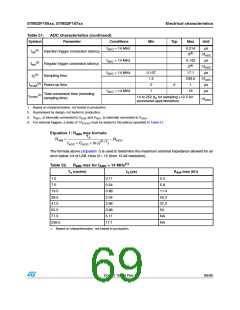
12-bit ADC characteristics
Unless otherwise specified, the parameters given in Table 51 are derived from tests
supply voltage
performed under the ambient temperature, f
conditions summarized in Table 9.
frequency and V
PCLK2
DDA
Note:
It is recommended to perform a calibration after each power-up.
Table 51. ADC characteristics
Symbol Parameter
Conditions
Min
Typ
Max
Unit
VDDA Power supply
2.4
2.4
3.6
VDDA
220(1)
14
V
V
VREF+ Positive reference voltage
IVREF Current on the VREF input pin
160(1)
µA
fADC ADC clock frequency
0.6
MHz
MHz
kHz
1/fADC
(2)
fS
Sampling rate
0.05
1
fADC = 14 MHz
823
17
(2)
fTRIG
External trigger frequency
0 (VSSA or VREF-
tied to ground)
VAIN
Conversion voltage range(3)
External input impedance
VREF+
V
See Equation 1 and
Table 52 for details
(2)
RAIN
50
kY
(2)
(2)
RADC
CADC
Sampling switch resistance
1
8
kY
pF
Internal sample and hold capacitor
fADC = 14 MHz
5.9
83
µs
(2)
tCAL
Calibration time
1/fADC
68/95
Doc ID 15274 Rev 4

 STMICROELECTRONICS [ ST ]