Electrical characteristics
STM32F405xx, STM32F407xx
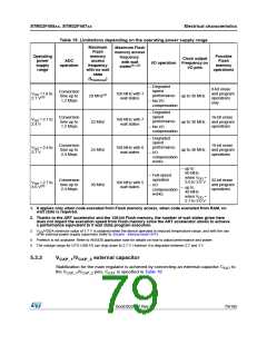
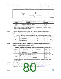
Figure 23. External capacitor C
EXT
C
ESR
R Leak
MS19044V2
1. Legend: ESR is the equivalent series resistance.
(1)
Table 16. V
/V
operating conditions
CAP_1 CAP_2
Symbol
Parameter
Conditions
CEXT
ESR
Capacitance of external capacitor
ESR of external capacitor
2.2 µF
< 2 Ω
1. When bypassing the voltage regulator, the two 2.2 µF VCAP capacitors are not required and should be
replaced by two 100 nF decoupling capacitors.
5.3.3
Operating conditions at power-up / power-down (regulator ON)
Subject to general operating conditions for T .
A
Table 17. Operating conditions at power-up / power-down (regulator ON)
Symbol
Parameter
VDD rise time rate
VDD fall time rate
Min
Max
Unit
20
20
∞
∞
tVDD
µs/V
5.3.4
Operating conditions at power-up / power-down (regulator OFF)
Subject to general operating conditions for T .
A
(1)
Table 18. Operating conditions at power-up / power-down (regulator OFF)
Symbol
Parameter
Conditions
Power-up
Min
Max Unit
VDD rise time rate
20
20
∞
∞
tVDD
V
DD fall time rate
Power-down
Power-up
VCAP_1 and VCAP_2 rise time
rate
µs/V
20
20
∞
tVCAP
VCAP_1 and VCAP_2 fall time
rate
Power-down
∞
1. To reset the internal logic at power-down, a reset must be applied on pin PA0 when VDD reach below
minimum value of V12
.
5.3.5
Embedded reset and power control block characteristics
The parameters given in Table 19 are derived from tests performed under ambient
temperature and V supply voltage conditions summarized in Table 14.
DD
80/185
DocID022152 Rev 4

 STMICROELECTRONICS [ ST ]