Electrical characteristics
STM32F405xx, STM32F407xx
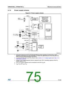
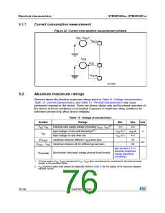
5.1.7
Current consumption measurement
Figure 22. Current consumption measurement scheme
I
_V
DD BAT
V
BAT
I
DD
V
DD
V
DDA
ai14126
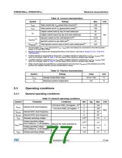
5.2
Absolute maximum ratings
Stresses above the absolute maximum ratings listed in Table 11: Voltage characteristics,
Table 12: Current characteristics, and Table 13: Thermal characteristics may cause
permanent damage to the device. These are stress ratings only and functional operation of
the device at these conditions is not implied. Exposure to maximum rating conditions for
extended periods may affect device reliability.
Table 11. Voltage characteristics
Symbol
DD–VSS
Ratings
Min
Max
Unit
(1)
V
External main supply voltage (including VDDA, VDD
Input voltage on five-volt tolerant pin(2)
Input voltage on any other pin
)
–0.3
4.0
VDD+4
4.0
VSS–0.3
V
VIN
|ΔVDDx
V
SS–0.3
|
Variations between different VDD power pins
Variations between all the different ground pins
-
-
50
mV
|VSSX − VSS
|
50
see Section 5.3.14:
Absolute maximum
ratings (electrical
sensitivity)
VESD(HBM)
Electrostatic discharge voltage (human body model)
1. All main power (VDD, VDDA) and ground (VSS, VSSA) pins must always be connected to the external power
supply, in the permitted range.
2. VIN maximum value must always be respected. Refer to Table 12 for the values of the maximum allowed
injected current.
76/185
DocID022152 Rev 4

 STMICROELECTRONICS [ ST ]