STM32F405xx, STM32F407xx
Electrical characteristics
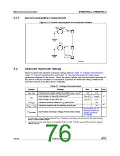
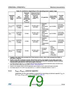
Table 15. Limitations depending on the operating power supply range
Maximum
Flash
memory
access
frequency
with no wait
state
Maximum Flash
memory access
frequency
Operating
power
supply
range
Possible
Flash
memory
operations
Clock output
I/O operation Frequency on
I/O pins
ADC
operation
with wait
states(1) (2)
(fFlashmax
)
– Degraded
speed
performance
up to 30 MHz
– No I/O
compensation
8-bit erase
and program
operations
only
Conversion
time up to
1.2 Msps
VDD =1.8 to
2.1 V(3)
160 MHz with 7
wait states
20 MHz(4)
– Degraded
speed
performance
Conversion
time up to
1.2 Msps
16-bit erase
and program
operations
VDD = 2.1 to
2.4 V
168 MHz with 7
wait states
22 MHz
up to 30 MHz
up to 48 MHz
– No I/O
compensation
– Degraded
speed
performance
Conversion
time up to
2.4 Msps
16-bit erase
and program
operations
VDD = 2.4 to
2.7 V
168 MHz with 6
wait states
24 MHz
– I/O
compensation
works
– up to
60 MHz
when VDD
– Full-speed
operation
=
Conversion
time up to
2.4 Msps
32-bit erase
and program
operations
3.0 to 3.6 V
VDD = 2.7 to
3.6 V(5)
168 MHz with 5
wait states
30 MHz
– I/O
compensation
works
– up to
48 MHz
when VDD
=
2.7 to 3.0 V
1. It applies only when code executed from Flash memory access, when code executed from RAM, no
wait state is required.
2. Thanks to the ART accelerator and the 128-bit Flash memory, the number of wait states given here
does not impact the execution speed from Flash memory since the ART accelerator allows to achieve
a performance equivalent to 0 wait state program execution.
3. VDD/VDDA minimum value of 1.7 V is obtained when the device operates in reduced temperature range, and with the use
of an external power supply supervisor (refer to Section : Internal reset OFF).
4. Prefetch is not available. Refer to AN3430 application note for details on how to adjust performance and power.
5. The voltage range for OTG USB FS can drop down to 2.7 V. However it is degraded between 2.7 and 3 V.
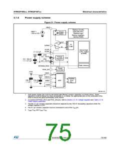
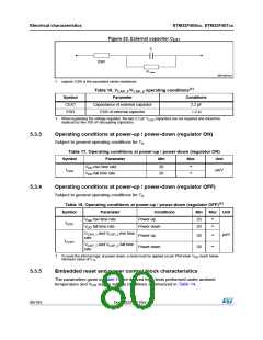
5.3.2
V
/V
external capacitor
CAP_1 CAP_2
Stabilization for the main regulator is achieved by connecting an external capacitor C
to
EXT
the V
/V
pins. C
is specified in Table 16.
EXT
CAP_1 CAP_2
DocID022152 Rev 4
79/185

 STMICROELECTRONICS [ ST ]