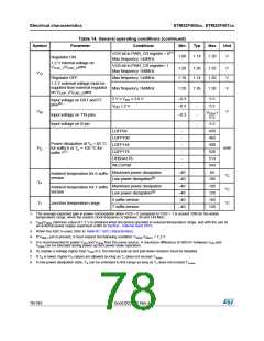
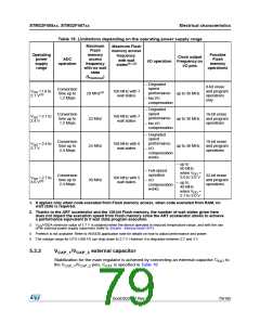
Electrical characteristics
STM32F405xx, STM32F407xx
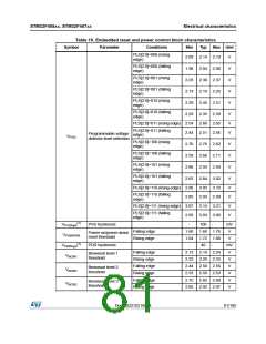
Table 19. Embedded reset and power control block characteristics (continued)
Symbol
Parameter
Conditions
Min
Typ Max Unit
(1)
VBORhyst
BOR hysteresis
-
100
1.5
-
mV
ms
(1)(2)
TRSTTEMPO
Reset temporization
0.5
3.0
InRush current on
voltage regulator
power-on (POR or
wakeup from Standby)
(1)
(1)
IRUSH
-
-
160
-
200
mA
µC
InRush energy on
voltage regulator
power-on (POR or
wakeup from Standby)
VDD = 1.8 V, TA = 105 °C,
IRUSH = 171 mA for 31 µs
ERUSH
5.4
1. Guaranteed by design, not tested in production.
2. The reset temporization is measured from the power-on (POR reset or wakeup from VBAT) to the instant
when first instruction is read by the user application code.
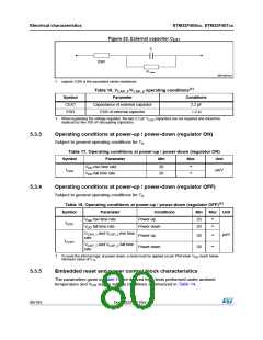
5.3.6
Supply current characteristics
The current consumption is a function of several parameters and factors such as the
operating voltage, ambient temperature, I/O pin loading, device software configuration,
operating frequencies, I/O pin switching rate, program location in memory and executed
binary code.
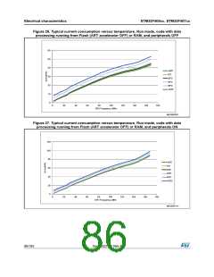
The current consumption is measured as described in Figure 22: Current consumption
measurement scheme.
All Run mode current consumption measurements given in this section are performed using
a CoreMark-compliant code.
Typical and maximum current consumption
The MCU is placed under the following conditions:
•
•
•
At startup, all I/O pins are configured as analog inputs by firmware.
All peripherals are disabled except if it is explicitly mentioned.
The Flash memory access time is adjusted to f
frequency (0 wait state from 0 to
HCLK
30 MHz, 1 wait state from 30 to 60 MHz, 2 wait states from 60 to 90 MHz, 3 wait states
from 90 to 120 MHz, 4 wait states from 120 to 150 MHz, and 5 wait states from 150 to
168 MHz).
•
•
When the peripherals are enabled HCLK is the system clock, f
= f
/4, and
PCLK1
HCLK
f
= f
/2, except is explicitly mentioned.
PCLK2
HCLK
The maximum values are obtained for V = 3.6 V and maximum ambient temperature
DD
(T ), and the typical values for T = 25 °C and V = 3.3 V unless otherwise specified.
A
A
DD
82/185
DocID022152 Rev 4

 STMICROELECTRONICS [ ST ]