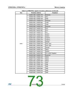
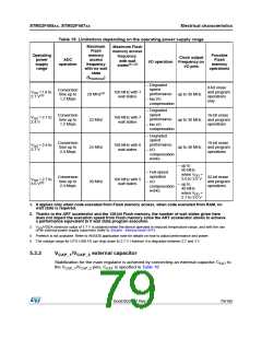
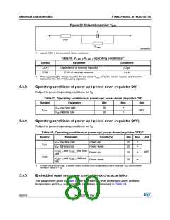
STM32F405xx, STM32F407xx
Symbol
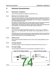
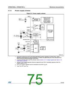
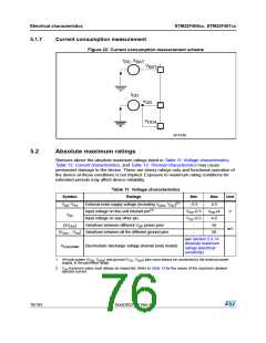
Electrical characteristics
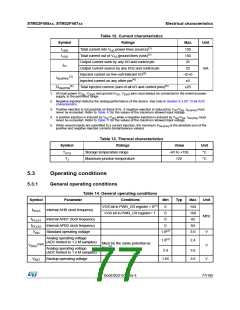
Table 12. Current characteristics
Ratings
Max.
Unit
IVDD
IVSS
Total current into VDD power lines (source)(1)
Total current out of VSS ground lines (sink)(1)
Output current sunk by any I/O and control pin
Output current source by any I/Os and control pin
Injected current on five-volt tolerant I/O(3)
Injected current on any other pin(4)
150
150
25
IIO
25
mA
–5/+0
±5
(2)
IINJ(PIN)
Total injected current (sum of all I/O and control pins)(5)
±25
(4)
ΣIINJ(PIN)
1. All main power (VDD, VDDA) and ground (VSS, VSSA) pins must always be connected to the external power
supply, in the permitted range.
2. Negative injection disturbs the analog performance of the device. See note in Section 5.3.20: 12-bit ADC
characteristics.
3. Positive injection is not possible on these I/Os. A negative injection is induced by VIN<VSS. IINJ(PIN) must
never be exceeded. Refer to Table 11 for the values of the maximum allowed input voltage.
4. A positive injection is induced by VIN>VDD while a negative injection is induced by VIN<VSS. IINJ(PIN) must
never be exceeded. Refer to Table 11 for the values of the maximum allowed input voltage.
5. When several inputs are submitted to a current injection, the maximum ΣIINJ(PIN) is the absolute sum of the
positive and negative injected currents (instantaneous values).
Table 13. Thermal characteristics
Symbol
Ratings
Value
Unit
TSTG
TJ
Storage temperature range
–65 to +150
125
°C
°C
Maximum junction temperature
5.3
Operating conditions
5.3.1
General operating conditions
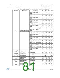
Table 14. General operating conditions
Symbol
Parameter
Conditions
Min
Typ
Max
Unit
VOS bit in PWR_CR register = 0(1)
VOS bit in PWR_CR register= 1
0
0
0
0
144
168
42
fHCLK
Internal AHB clock frequency
MHz
fPCLK1 Internal APB1 clock frequency
fPCLK2 Internal APB2 clock frequency
84
VDD
Standard operating voltage
1.8(2)
3.6
V
V
V
Analog operating voltage
(ADC limited to 1.2 M samples)
1.8(2)
2.4
Must be the same potential as
VDD
(3)(4)
VDDA
(5)
Analog operating voltage
(ADC limited to 1.4 M samples)
2.4
3.6
3.6
VBAT
Backup operating voltage
1.65
DocID022152 Rev 4
77/185

 STMICROELECTRONICS [ ST ]